概要
説明
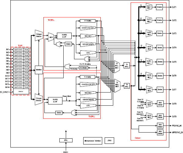
The 82V3390 is an integrated, single-chip solution for the Synchronous Equipment Timing Source for Stratum 3, Stratum 4E, Stratum 4, SMC, EEC-Option1, EEC-Option2 clocks in SONET / SDH / Synchronous Ethernet equipment, DWDM and Wireless base station. The device supports three types of input clock sources: recovered clock from STM-N or OC-n, PDH network synchronization timing and external synchronization reference timing. The device consists of T0 and T4 paths. The T0 path is a high quality and highly configurable path to provide system clock for node timing synchronization within a SONET / SDH / Synchronous Ethernet network. The T4 path is simpler and less configurable for equipment synchronization. The T4 path locks independently from the T0 path or locks to the T0 path. An input clock is automatically or manually selected for T0 and T4 each for DPLL locking. Both the T0 and T4 paths support three primary operating modes: Free-Run, Locked and Holdover. In Free-Run mode, the DPLL refers to the master clock. In Locked mode, the DPLL locks to the selected input clock. In Holdover mode, the DPLL resorts to the frequency data acquired in Locked mode. Whatever the operating mode is, the DPLL gives a stable performance without being affected by operating conditions or silicon process variations. If the DPLL outputs are processed by T0/T4 APLL, the outputs of the device will be in a better jitter/wander performance. The device provides programmable DPLL bandwidths: 0.5 mHz to 560 Hz in 19 steps and damping factors: 1.2 to 20 in 5 steps. Different settings cover all SONET / SDH clock synchronization requirements. A high stable input is required for the master clock in different applications. The master clock is used as a reference clock for all the internal circuits in the device. It can be calibrated within ±741 ppm. All the read/write registers are accessed through a microprocessor interface. The device supports six microprocessor interface modes: EPROM, Multiplexed, Intel, Motorola, I2C and Serial. In general, the device can be used in Master/Slave application. In this application, two devices should be used together to enable system protection against single chip failure.
特長
- Single PLL chip:
- Features 0.5 mHz to 560 Hz bandwidth
- Provides node clock for ITU-T G.8261/G.8262 Synchronous Ethernet (SyncE)
- Exceeds GR-253-CORE and ITU-T G.813 jitter generation requirements
- Provides node clocks for Cellular and WLL base-station (GSM and 3G networks)
- Provides clocks for DSL access concentrators (DSLAM), especially for Japan TCM-ISDN network timing based ADSL equipments
- Provides clocks for 1 Gigabit and 10 Gigabit Ethernet applications
- Provides an integrated single-chip solution for Synchronous Equipment Timing Source, including Stratum 3, Stratum 4E, Stratum 4, SMC, EEC-Option 1 and EEC-Option 2 Clocks
- Provides 156.25 MHz clock for 10 Gig Ethernet Application, with less than 0.7 ps of RMS Phase Jitter (12 kHz - 20 MHz)
- Employs PLL architecture to feature excellent jitter performance and minimize the number of the external components
- Integrates T0 DPLL and T4 DPLL
- T4 DPLL locks independently or locks to T0 DPLL
- Supports Forced or Automatic operating mode switch controlled by an internal state machine. It supports Free- Run, Locked and Holdover modes
- Supports programmable DPLL bandwidth (0.5 mHz to 560 Hz in 19 steps) and damping factor (1.2 to 20 in 5 steps)
- Supports 1.1X10⁻⁵ ppm absolute holdover accuracy and 4.4X10⁻⁸ ppm instantaneous holdover accuracy
- Supports hitless reference switching to minimize phase transients on T0 DPLL output to be no more than 0.61 ns
- Supports phase absorption when phase-time changes on T0 selected input clock are greater than a programmable limit over an interval of less than 0.1 seconds
- Supports programmable input-to-output phase offset adjustment
- Limits the phase and frequency offset of the outputs
- Provides OUT1~OUT7 output clock frequencies covering from 2 kHz to 625MHz
- Includes 125 MHz and 156.25 MHz for CMOS outputs
- Includes 125 MHz, 156.25 MHz, 312.5 MHz and 625 MHz for differential outputs
- Provides OUT8 for composite clocks and OUT9 for 1.544 MHz/ 2.048 MHz (BITS/SSU)
- Provides IN1 and IN2 for composite clocks
- Provides IN3~IN14 input clock frequencies covering from 2 kHz to 625 MHz
- Includes 125 MHz and 156.25 MHz for CMOS inputs
- Includes 156.25 MHz, 312.5 MHz and 625 MHz for differential inputs
- Supports manual and automatic selected input clock switch
- Supports automatic hitless selected input clock switch on clock failure
- Supports three types of input clock sources: recovered clock from STM-N or OC-n, PDH network synchronization timing and external synchronization reference timing
- Provides a 2 kHz, 4 kHz or 8 kHz frame sync input signal, and a 2 kHz and an 8 kHz frame sync output signals
- Provides output clocks for BITS, GPS, 3G, GSM, etc.
- Supports AMI, PECL/LVDS and CMOS input/output technologies
- Supports master clock calibration
- Supports Master/Slave application (two chips used together) to enable system protection against single chip failure
- Supports Telcordia GR-1244-CORE, Telcordia GR-253-CORE, ITU-T G.812, ITU-T G.8262. ITU-T G.813 and ITU-T G.783 Recommendations
- Multiple microprocessor interface modes: EPROM, Multiplexed, Intel, Motorola, I2C and Serial
- IEEE 1149.1 JTAG Boundary Scan
- Single 3.3 V operation with 5 V tolerant CMOS I/Os
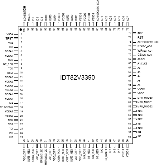
- 100-pin TQFP package, green package options available
製品比較
アプリケーション
ドキュメント
|
|
|
|
|---|---|---|
| 分類 | タイトル | 日時 |
| データシート | PDF 1.49 MB | |
| EOL通知 | PDF 938 KB | |
| EOL通知 | PDF 909 KB | |
| 製品変更通知 | PDF 32 KB | |
| 製品変更通知 | PDF 567 KB | |
5 items
|
||
設計・開発
モデル
ECADモデル
[製品選択]テーブル内の製品名をクリックするとSamacSysが提供する回路図シンボル、PCBフットプリント、3D CADモデルがご確認いただけます。 お探しのシンボルやモデルが見つからない場合、Webサイトから直接リクエストできます。
| TQFP | 100 | C | Yes | Tray | ||
| TQFP | 100 | C | Yes | Reel |

Tips for Using This Parametric Table:
- Hide Filters button in header: Collapse or expands filters
- Column sort buttons in header: Sort Column alphabetically / numerically descending or ascending
- Reset button in header: Reset all filters to the page default
- Full Screen button in header: Expand the table to full screen view (user must close out of full screen before they can interact with rest of page)
- Export button in header: Export the filtered results of the table to an Excel document
- Filter parts search bar in header: Type to filter table results by part number
- Hide column button in column headers: Select to hide columns in table
- AND / OR toggle switches in header: Toggles the logic of this particular filter to be “AND” or “OR” logic for filtering results
- Multiselect checkboxes at beginning of each row in table: Select these checkboxes to compare products against each other
- Document icon next to product name in row: View the featured document for this product
- Chip icon next to the right of the document icon in row: View the block diagram for this product
- Cart icon to the right of the chip icon: Indicates that samples are available for this product