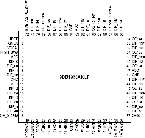
概要
説明
The 9DB1933 zero-delay buffer supports PCIe Gen3 requirements, while being backwards compatible to PCIe Gen2 and Gen1. The 9DB1933 is driven by a differential SRC output pair from an IDT 932S421, 932SQ420, or equivalent, main clock generator. It attenuates jitter on the input clock and has a selectable PLL bandwidth to maximize performance in systems with or without Spread-Spectrum clocking.

特長
- 19 - 0.7 V current mode differential HCSL output pairs
- 8 Selectable SMBus Addresses/Multiple devices can share the same SMBus Segment
- 11 dedicated and 3 group OE# pins/Hardware control of the outputs
- PLL or bypass mode/PLL can dejitter incoming clock
- Selectable PLL bandwidth/minimizes jitter peaking in downstream PLL's
- Spread spectrum compatible, tracks spreading input clock for low EMI
- SMBus Interface, unused outputs can be disabled
- Supports undriven differential outputs in Power Down mode for power management
- Cycle-to-cycle jitter <50 ps
- Output-to-output skew < 150 ps
- PCIe Gen3 phase jitter < 1.0 ps RMS
製品比較
アプリケーション
設計・開発
モデル
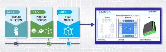
ECADモデル
[製品選択]テーブル内の製品名をクリックするとSamacSysが提供する回路図シンボル、PCBフットプリント、3D CADモデルがご確認いただけます。 お探しのシンボルやモデルが見つからない場合、Webサイトから直接リクエストできます。
| VFQFPN | 72 | C | Yes | Tray | ||
| VFQFPN | 72 | C | Yes | Reel |

Tips for Using This Parametric Table:
- Hide Filters button in header: Collapse or expands filters
- Column sort buttons in header: Sort Column alphabetically / numerically descending or ascending
- Reset button in header: Reset all filters to the page default
- Full Screen button in header: Expand the table to full screen view (user must close out of full screen before they can interact with rest of page)
- Export button in header: Export the filtered results of the table to an Excel document
- Filter parts search bar in header: Type to filter table results by part number
- Hide column button in column headers: Select to hide columns in table
- AND / OR toggle switches in header: Toggles the logic of this particular filter to be “AND” or “OR” logic for filtering results
- Multiselect checkboxes at beginning of each row in table: Select these checkboxes to compare products against each other
- Document icon next to product name in row: View the featured document for this product
- Chip icon next to the right of the document icon in row: View the block diagram for this product
- Cart icon to the right of the chip icon: Indicates that samples are available for this product
ビデオ&トレーニング
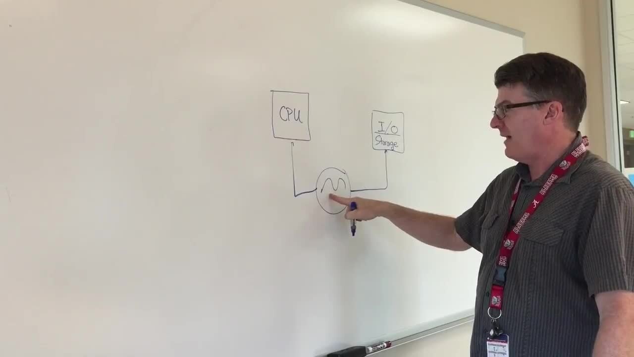
This is the first video in our PCIe series. In this video, we define PCIe architectures, focusing on common and separate clock architectures. Watch the rest of the video series below where Ron will cover the impact of different timing architectures.
Watch the Video Series Below
ニュース&ブログ
| ブログ | 2022年4月14日 | ||
| ブログ | 2018年5月22日 | ||
| ニュース | 2018年4月30日 |