概要
説明
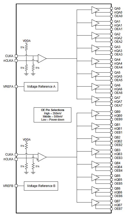
The 8P34S2108-1 is a differential dual 1:8 LVDS output 1.8V/2.5V fanout buffer that boasts high performance and low power consumption. It is engineered to support fail-safe operation and is specifically designed for the fanout of high-frequency clock and data signals with very low additive phase noise. The device comprises two independent buffer channels, and each of these channels has eight outputs with low skew. High isolation between the channels ensures minimal noise coupling.
The 8P34S2108-1 shines in clock distribution applications that require well-defined performance and repeatability due to its guaranteed output-to-output and part-to-part skew characteristics. The device can operate using a 1.8V or 2.5V power supply. Its integrated bias voltage references allow for the easy interfacing of AC-coupled signals with the device's inputs.
The 8P34S2108-1 had the individual OE/Swing control pin for each output, which provides excellent control over both swing and output enable functions.
特長
- Dual 1:8 low skew, low additive jitter LVDS fanout buffers
- Individual OE/Swing control pin for each output
- Matched AC characteristics across both channels
- High isolation between channels
- Both differential CLKA, nCLKA and CLKB, nCLKB inputs accept LVDS, LVPECL, and single-ended LVCMOS levels
- Maximum input clock frequency: 2GHz
- Output amplitudes: 350mV, 500mV or disable (selectable)
- Output skew: 20ps typical
- Low additive phase jitter, RMS: 50fs typical
(fREF = 156.25MHz, 12kHz to 20MHz) - Full 1.8V and 2.5V supply voltage mode
- Low device current consumption (IDD)
- Lead-free (RoHS 6), 64-lead VFQFPN packaging
- -40 °C to +85 °C ambient operating temperature
- Supports case temperature up to +105 °C
製品比較
アプリケーション
アプリケーション
- 4G and 5G radio unit (RU) and distributed unit (DU) systems
- Ethernet switches/routers
- Medical imaging
- Professional audio and video
- Data centers and servers
設計・開発
モデル
ECADモデル
[製品選択]テーブル内の製品名をクリックするとSamacSysが提供する回路図シンボル、PCBフットプリント、3D CADモデルがご確認いただけます。 お探しのシンボルやモデルが見つからない場合、Webサイトから直接リクエストできます。
| VFQFPN | 48 | I | 0 | Yes | Tray | サンプルを入手, | |
| VFQFPN | 64 | I | 1 | Yes | Reel | ||
| VFQFPN | 64 | I | 2 | Yes | Reel |

Tips for Using This Parametric Table:
- Hide Filters button in header: Collapse or expands filters
- Column sort buttons in header: Sort Column alphabetically / numerically descending or ascending
- Reset button in header: Reset all filters to the page default
- Full Screen button in header: Expand the table to full screen view (user must close out of full screen before they can interact with rest of page)
- Export button in header: Export the filtered results of the table to an Excel document
- Filter parts search bar in header: Type to filter table results by part number
- Hide column button in column headers: Select to hide columns in table
- AND / OR toggle switches in header: Toggles the logic of this particular filter to be “AND” or “OR” logic for filtering results
- Multiselect checkboxes at beginning of each row in table: Select these checkboxes to compare products against each other
- Document icon next to product name in row: View the featured document for this product
- Chip icon next to the right of the document icon in row: View the block diagram for this product
- Cart icon to the right of the chip icon: Indicates that samples are available for this product