Overview
Description
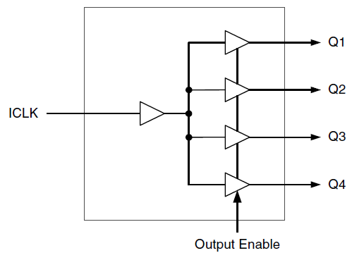
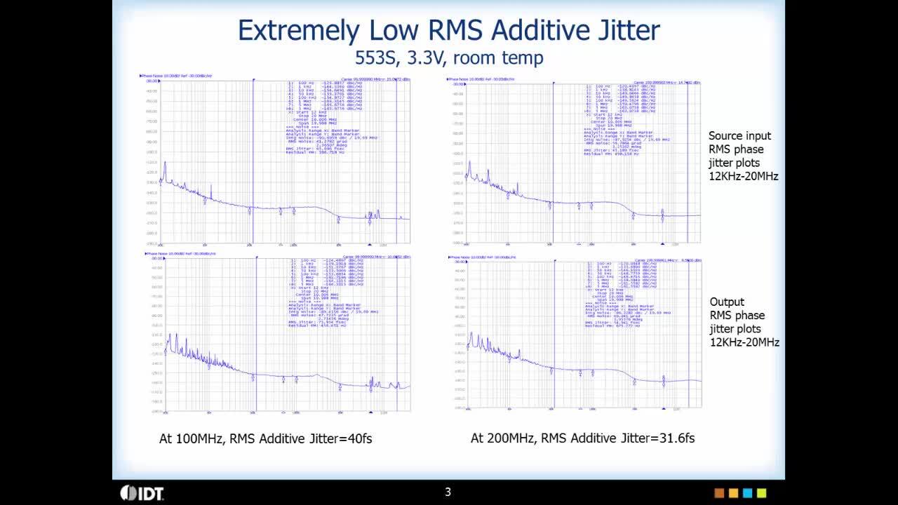
The 651S is a low cost, high-speed single input to four output LVCMOS clock buffer. The 651S has best in class Additive Phase Jitter of sub 50 fsec.


Features
- Low additive phase jitter RMS: 50 fs
- Extremely low skew outputs (50 ps)
- Low cost clock buffer
- Packaged in 8-pin SOIC and 8-pin DFN, Pb-free
- Input / Output clock frequency up to 200 MHz
- Non-inverting output clock
- Ideal for networking clocks
- Operating Voltages: 1.8 V to 3.3 V
- Output Enable mode tri-states outputs
- Advanced, low power CMOS process
- Extended temperature range (-40°C to +105°C)
Comparison
Applications
Documentation
= Featured Documentation
Log in required to subscribe
|
|
|
|
|---|---|---|
| Type | Title | Date |
| Datasheet | PDF 305 KB | |
| Application Note | PDF 187 KB | |
| Overview | PDF 217 KB | |
| Product Change Notice | PDF 268 KB | |
| Product Change Notice | PDF 611 KB | |
| Product Change Notice | PDF 611 KB | |
| Application Note | PDF 495 KB | |
| Application Note | PDF 442 KB | |
| Application Note | PDF 565 KB | |
9 items
|
||
Design & Development
Models
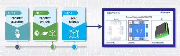
ECAD Models
Schematic symbols, PCB footprints, and 3D CAD models from SamacSys can be found by clicking on products in the Product Options table. If a symbol or model isn't available, it can be requested directly from the website.
Processing table
| COL | 8 | I | Yes | Cut Tape | 1 | 1.803 | Get Samples, | |
| COL | 8 | I | Yes | Reel | 1 | 1.697 | ||
| SOIC | 8 | I | Yes | Tube | 1 | 2.012 | Get Samples, | |
| SOIC | 8 | I | Yes | Reel | 1 | 1.697 |
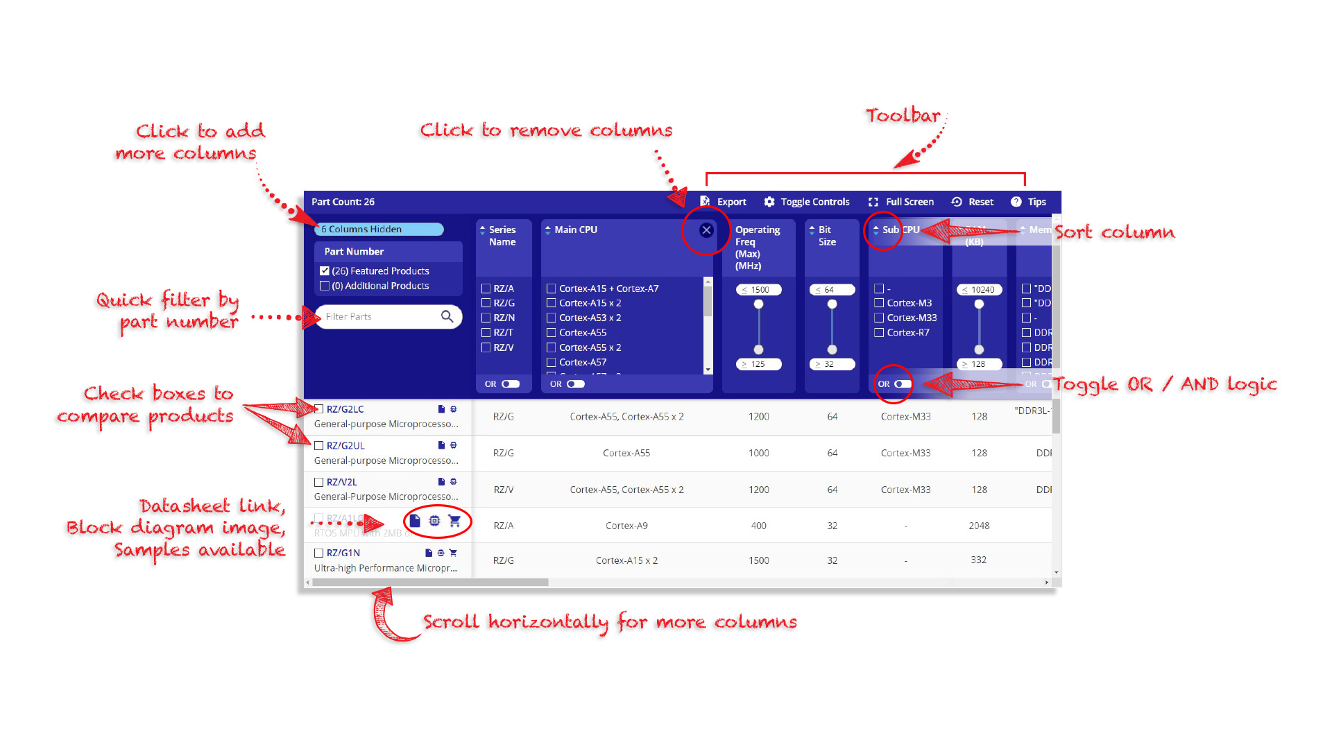
Tips for Using This Parametric Table:
- Hide Filters button in header: Collapse or expands filters
- Column sort buttons in header: Sort Column alphabetically / numerically descending or ascending
- Reset button in header: Reset all filters to the page default
- Full Screen button in header: Expand the table to full screen view (user must close out of full screen before they can interact with rest of page)
- Export button in header: Export the filtered results of the table to an Excel document
- Filter parts search bar in header: Type to filter table results by part number
- Hide column button in column headers: Select to hide columns in table
- AND / OR toggle switches in header: Toggles the logic of this particular filter to be “AND” or “OR” logic for filtering results
- Multiselect checkboxes at beginning of each row in table: Select these checkboxes to compare products against each other
- Document icon next to product name in row: View the featured document for this product
- Chip icon next to the right of the document icon in row: View the block diagram for this product
- Cart icon to the right of the chip icon: Indicates that samples are available for this product
Videos & Training
Low-jitter LVCMOS Fanout Clock Buffers by IDT
This video overviews the LVCMOS Fanout Buffers, showcasing their best-in-class performance with extremely low phase jitter, minimal output skew, and low power consumption, along with other competitive features.
Video List