概要
説明
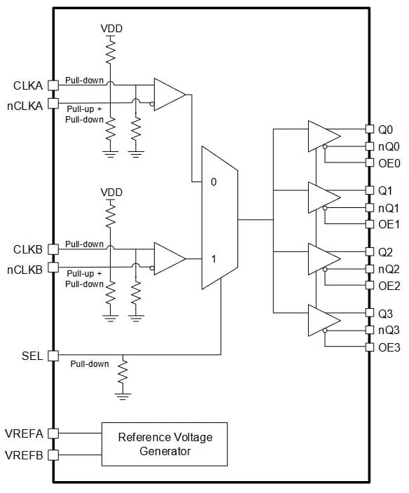
The 8P34S1204 is a high-performance differential LVDS fanout buffer. The device is designed for the fanout of 1PPS signals or high-frequency, very low additive phase-noise clock and data signals.
The 8P34S1204 supports fail-safe operation and is characterized to operate from a 1.8V or 2.5V power supply. Guaranteed output-to-output and part-to-part skew characteristics make the 8P34S1204 ideal for those clock distribution applications demanding well-defined performance and repeatability. Two selectable differential inputs and four low skew outputs are available. The integrated bias voltage reference enables easy interfacing of single-ended signals to the differential device input. The device is optimized for low power consumption and low additive phase noise.
The 8P34S1204-1 has an individual OE control pin for each output, which provides excellent control over the output enable functions.
特長
- Four low skew, low additive jitter LVDS output pairs
- Individual OE control pin for each output
- Two selectable, differential clock input pairs
- Differential CLK, nCLK pairs can accept the following differential input levels: LVDS, CML
- Maximum input clock frequency: 2GHz
- LVCMOS/LVTTL interface levels for the control input select pin
- Output skew: 10ps (typical)
- Propagation delay: 475ps (maximum)
- Low propagation delay variation across temperature for 1PPS applications
- Low additive phase jitter, RMS; fREF = 156.25MHz, VPP = 1V, 12kHz – 20MHz: 50fs (typical)
- Device current consumption (IDD): 100mA (typical)
- Full 1.8V or 2.5V supply voltage
- Lead-free (RoHS 6), 28-Lead VFQFPN package
- -40 °C to 85 °C ambient operating temperature
- Supports case temperature up to +105 °C
製品比較
アプリケーション
アプリケーション
- 4G and 5G radio unit (RU) and distributed unit (DU) systems
- Ethernet switches/routers
- Medical imaging
- Professional audio and video
- Data centers and servers
設計・開発
モデル
ECADモデル
[製品選択]テーブル内の製品名をクリックするとSamacSysが提供する回路図シンボル、PCBフットプリント、3D CADモデルがご確認いただけます。 お探しのシンボルやモデルが見つからない場合、Webサイトから直接リクエストできます。
| VFQFPN | 28 | I | Yes | Tray | サンプルを入手, | |
| VFQFPN | 28 | I | Yes | Reel | ||
| VFQFPN | 28 | I | Yes | Reel |

Tips for Using This Parametric Table:
- Hide Filters button in header: Collapse or expands filters
- Column sort buttons in header: Sort Column alphabetically / numerically descending or ascending
- Reset button in header: Reset all filters to the page default
- Full Screen button in header: Expand the table to full screen view (user must close out of full screen before they can interact with rest of page)
- Export button in header: Export the filtered results of the table to an Excel document
- Filter parts search bar in header: Type to filter table results by part number
- Hide column button in column headers: Select to hide columns in table
- AND / OR toggle switches in header: Toggles the logic of this particular filter to be “AND” or “OR” logic for filtering results
- Multiselect checkboxes at beginning of each row in table: Select these checkboxes to compare products against each other
- Document icon next to product name in row: View the featured document for this product
- Chip icon next to the right of the document icon in row: View the block diagram for this product
- Cart icon to the right of the chip icon: Indicates that samples are available for this product