概要
説明

特長
-
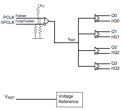
Four low skew, low additive jitter LVPECL differential output pairs
-
Differential LVPECL input pair can accept the following differential input levels: LVDS, LVPECL, CML
-
Differential PCLKx pairs can also accept single-ended LVCMOS levels. See the Applications section Writing the Differential Input Levels to Accept Single-ended Levels (Figures 1 and 2)
-
Maximum input clock frequency: 2GHz
-
LVCMOS interface levels for the control input (input select)
-
Output skew: 5ps (typical)
-
Propagation delay: 320ps (maximum)
-
Low additive phase jitter, RMS; fREF = 156.25MHz, VPP = 1V, 12kHz - 20MHz: 40fs (maximum)
-
Maximum device current consumption (IEE): 60mA (maximum)
-
Full 3.3V or 2.5V supply voltage
-
Lead-free (RoHS 6) packaging
-
-40°C to 85°C ambient operating temperature
製品比較
アプリケーション
設計・開発
ソフトウェア/ツール
モデル
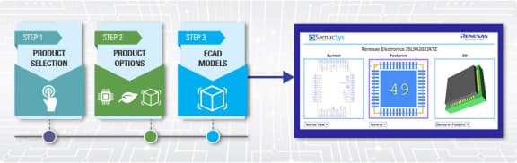
ECADモデル
[製品選択]テーブル内の製品名をクリックするとSamacSysが提供する回路図シンボル、PCBフットプリント、3D CADモデルがご確認いただけます。 お探しのシンボルやモデルが見つからない場合、Webサイトから直接リクエストできます。
| VFQFPN | 16 | I | Yes | Tray | 3 | 4.43 | サンプルを入手, | |
| VFQFPN | 16 | I | Yes | Reel | 3 | 3.859 |

Tips for Using This Parametric Table:
- Hide Filters button in header: Collapse or expands filters
- Column sort buttons in header: Sort Column alphabetically / numerically descending or ascending
- Reset button in header: Reset all filters to the page default
- Full Screen button in header: Expand the table to full screen view (user must close out of full screen before they can interact with rest of page)
- Export button in header: Export the filtered results of the table to an Excel document
- Filter parts search bar in header: Type to filter table results by part number
- Hide column button in column headers: Select to hide columns in table
- AND / OR toggle switches in header: Toggles the logic of this particular filter to be “AND” or “OR” logic for filtering results
- Multiselect checkboxes at beginning of each row in table: Select these checkboxes to compare products against each other
- Document icon next to product name in row: View the featured document for this product
- Chip icon next to the right of the document icon in row: View the block diagram for this product
- Cart icon to the right of the chip icon: Indicates that samples are available for this product
ビデオ&トレーニング
Description
Overview of IDT's 8LSVP (LVPECL) and 8SLVD (LVDS) families of low-jitter fanout buffers from IDT. Fanout buffers are a useful building block of many clock trees, providing signal buffering and multiple low-skew copies of the input signal. IDT's high-performance, low additive phase noise, differential clock fan-out buffers offer up to 2 GHz clock operation, low additive phase jitter (12kHz - 20MHz) of 50 to 100 femtoseconds RMS max, fast output rise & fall times (less than 150ps), and single and dual channel functions (dual: matched propagation delay). Presented by Baljit Chandhoke, Product Marketing Manager at Integrated Device Technology, Inc. To learn more about IDT's industry-leading portfolio of fanout buffers, visit Renesas's RF Buffer page.
Transcript