概要
説明
The 5P83905 is a high-performance, 1-to-6 crystal input to LVCMOS fanout buffer with output enable pins. This device accepts a fundamental mode crystal from 10 MHz to 40 MHz and outputs LVCMOS clocks with best-in-class phase noise performance.
The 5P83905 features a synchronous glitch-free Output Enable function to eliminate any intermediate incorrect output clock cycles when enabling or disabling outputs. It comes in standard TSSOP packages or small QFN packages and can operate from 1.8 V to 3.3 V supplies.


特長
- Six copies of LVCMOS output clocks with best-in-class phase noise performance
- Phase Noise:
Offset Noise Power (3.3 V)- 100 Hz: -131 dBc/Hz
- 1 KHz: -145 dBc/Hz
- 10 KHz: -154 dBc/Hz
- 100 KHz: -161 dBc/Hz
- Operating power supply modes:
- Full 3.3 V, 2.5 V, 1.8 V
- Mixed 3.3 V core / 2.5 V output operating supply
- Mixed 3.3 V core / 1.8 V output operating supply
- Mixed 2.5 V core / 1.8 V output operating supply
- Crystal Oscillator Interface
- Synchronous Output Enable
- Packaged in 16-pin TSSOP and QFN packages
- Extended temperature range (-40°C to +105°C)
製品比較
アプリケーション
ドキュメント
= ピックアップ
ログイン後、ご登録が可能となります。
|
|
|
|
|---|---|---|
| 分類 | タイトル | 日時 |
| データシート | PDF 459 KB | |
| アプリケーションノート | PDF 187 KB | |
| 概要 | PDF 217 KB | |
| 製品変更通知 | PDF 268 KB | |
| 概要 | PDF 252 KB | |
| アプリケーションノート | PDF 495 KB | |
| アプリケーションノート | PDF 442 KB | |
| アプリケーションノート | PDF 565 KB | |
8 items
|
||
設計・開発
モデル
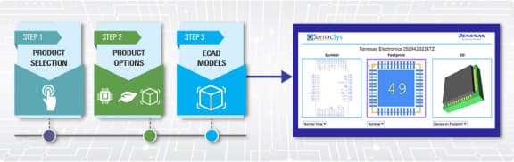
ECADモデル
[製品選択]テーブル内の製品名をクリックするとSamacSysが提供する回路図シンボル、PCBフットプリント、3D CADモデルがご確認いただけます。 お探しのシンボルやモデルが見つからない場合、Webサイトから直接リクエストできます。
Processing table

Tips for Using This Parametric Table:
- Hide Filters button in header: Collapse or expands filters
- Column sort buttons in header: Sort Column alphabetically / numerically descending or ascending
- Reset button in header: Reset all filters to the page default
- Full Screen button in header: Expand the table to full screen view (user must close out of full screen before they can interact with rest of page)
- Export button in header: Export the filtered results of the table to an Excel document
- Filter parts search bar in header: Type to filter table results by part number
- Hide column button in column headers: Select to hide columns in table
- AND / OR toggle switches in header: Toggles the logic of this particular filter to be “AND” or “OR” logic for filtering results
- Multiselect checkboxes at beginning of each row in table: Select these checkboxes to compare products against each other
- Document icon next to product name in row: View the featured document for this product
- Chip icon next to the right of the document icon in row: View the block diagram for this product
- Cart icon to the right of the chip icon: Indicates that samples are available for this product
ビデオ&トレーニング
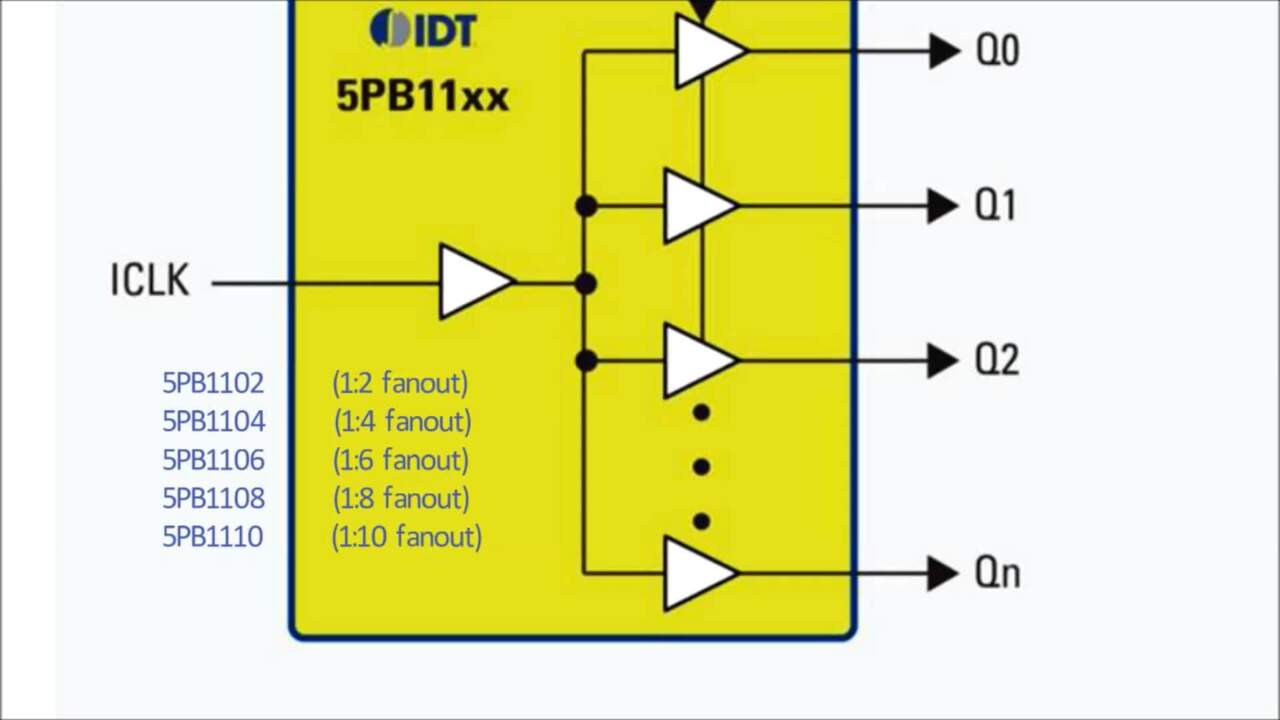
5PB11xx Ultra Low Jitter LVCMOS Buffers
This video provides an overview of the LVCMOS High Performance Clock Buffer Family, highlighting their key features and capabilities.
Video List
ニュース&ブログ
| IDT社が超低ジッターのLVCMOSクロックバッファ製品ファミリーを開発 | ニュース | 2015年3月30日 |