Nowadays, one of the most significant market challenges is to combine a variety of functions in a single chip to minimize the size of the devices, while providing high flexibility, efficiency, and best quality for signal processing and data management. The Renesas AnalogPAK™ SLG47011 is a great solution to combat these challenges.
Let's start from the basics - AnalogPAK is a relatively new sub-family of a wide family of GreenPAK™ Programmable Mixed-Signal Products with embedded high-performance analog blocks that can be configured and controlled by customer-defined logic functions to implement various scenarios. All macrocells are packed in one IC to achieve a high level of integration of common analog and digital components. The SLG47011 represents a significant milestone in the evolution of GreenPAK technology, marking a new era in programmable mixed-signal ICs. This latest chip builds upon the foundational principles of GreenPAK while introducing advanced features that dramatically expand its capabilities, setting a new standard for flexibility, performance, and integration in mixed-signal design.
Using the SLG47011 enables the performance of much more complicated designs than ever before. Engineers can offload or extend the performance of MCUs with SLG47011's new blocks such as Programmable Gain Amplifier (PGA), Analog-to-Digital Converter (ADC), Digital-to-Analog Converter (DAC), configuring A-D and D-A conversion, filtering, data storage, gain and offset compensation, and many more. Analog blocks plus GreenPAK configurable logic can easily replace complex AFEs with MCUs. For better energy-saving, there are new flexible user-defined power-saving modes for all macrocells. In Sleep mode, the chip consumes only ~0.6µA. As always, the GreenPAK family provides a tiny package product at a low cost for your mixed-signal project.
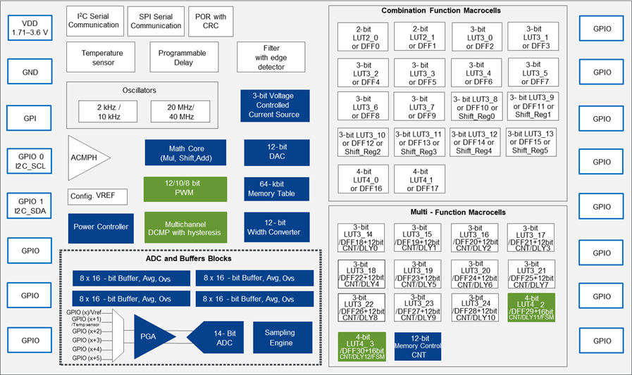
Below you can see a block diagram illustrating the internal structure of the SLG47011.

As can be seen from the diagram above, in addition to the usual GreenPAK fully configurable blocks such as LUTs, flip-flops, shift registers, timers, counters, and delays, the SLG47011 also has some new (blue) and improved (green) blocks.
Thanks to all these blocks, SLG47011 supports a wide range of applications such as HART modem, sensor interfacing (thermocouple interface with cold junction compensation, bridge sensors interface with gain and offset error compensation, current source as a power for sensor, internal temperature, and Vref (Vcc) sensing), current/voltage/power/temperature monitor and protection, capacitive sensor button, address RGB LEDs control, MPPT controller, and many others.
Let's take a look at the chip structure that makes this all possible, starting from the heart of the chip – PGA, ADC, and buffer blocks. A highly configurable low offset PGA allows users to select different amplifier modes and configurations that better suit input signal requirements.
The next weighty block is the cutting-edge 14-bit successive approximation register Analog-to-Digital Converter (SAR ADC) macrocell, delivering lightning-fast sampling rates of up to 1Msps in 14-bit mode and 2.35Msps in 8-bit mode. With features like parallel data output, auto-calibration, and selectable clock sources, it offers unparalleled precision and versatility for your signal processing needs.
Unleash the power of our chip's four versatile Data Buffers, customizable to store or process data from ADC or CNT/DLY sources. With selectable lengths and initial data settings, users can seamlessly tailor their experience, whether in Storage, Moving Average, or Oversampling modes, for incomparable operation.
Now, let's switch to the memory of our SLG47011. Memory Table macrocell is a memory block that houses 4096 12-bit words with a 12-bit address and data port. Customers can choose between RAM mode for ADC data buffering and external transfers via I²C/SPI, and ROM mode for rapid access to pre-programmed data arrays, enabling efficient function implementation and swift linearization without computational delays.
The SLG47011 has one 12-bit Width Converter macrocell designed to provide data from the memory table macrocell to the connection matrix. Choose your preferred output format: 12-bit parallel output, three 4-bit words, six 2-bit words, or a serial bit stream, granting unparalleled flexibility to suit your application needs.
Now we've received, amplified, sampled, and stored a lot of data. It already sounds great; however, SLG47011 has yet one more trick up its sleeve - the MathCore block. This Mathematical Core block supports four mathematical operations: addition, subtraction, multiplication, division (right shift), and their combinations. Input sources for the MathCore can be ADC channels, memory table output, data buffer outputs, or constants from registers.
The designers of this chip did not stop there and decided to add an improved Multichannel Digital Comparator macrocell with Hysteresis (DCMP). It compares up to four digital channels with synchronous or sequential result appearance. It is also possible to choose continuous sampling or one-time sequential sampling.
In addition to the blocks described above, there are also a PWM block, a 12-bit DAC, a power controller, and a large set of logic (LUT, flip-flops, counters, delays, and so on).
Elevate your signal processing and data management applications with our SLG47011, the ultimate IC for diverse solutions. By consolidating multiple functions onto a single chip, it streamlines design, minimizes board size, cuts power consumption, and slashes component costs. Experience the epitome of efficiency and innovation, empowering your projects to reach new heights of performance and cost-effectiveness.
Visit renesas.com/slg47011 to get more information, or order a kit to begin evaluation.
