
High-performance AI data centers are reshaping semiconductor design and investment trajectories like no technology we've seen. As recently as 2022, spending on AI infrastructure was in the vicinity of $15 billion. This year, expenditures could easily top $60 billion. Yes, that sucking sound you hear is the oxygen being pulled from every investment plan and breathed into data centers.
We are clearly operating in an era of unprecedented artificial intelligence capital outlays – notwithstanding the potential impact of newcomers like DeepSeek. But while high-performance computing (HPC) processors from Nvidia, AMD, and others are busy stealing the limelight, the high-bandwidth memory that stores training and inference models is having its day too – with 2024 DRAM revenue setting a record of nearly $116 billion.
Data center servers are driving a continuous increase in CPU core count, which requires more memory capacity to make higher-bandwidth data available to each processor core. But the laws of physics are quickly catching up. A CPU signal can only go so fast and far. That's where memory interface devices such as register-clock drivers (RCDs) and data buffers come into play. By allowing the clock, command, address, and data signals to be re-driven with much-improved signal integrity, these interfaces enable the entire memory subsystem to scale in speed and capacity.
Today, RCD empowers registered DIMMs (RDIMMs) to operate up to 8 Giga Transfers per Second (GT/s). Most data center servers use RDIMMs, although some HPC systems need even greater memory subsystem performance.
Memory Interfaces Further Accelerate DRAM and Processor Performance
Notable for the vital role it plays in data center server systems, DRAM architecture hasn't actually changed dramatically over the past three decades. Increases in density, speed, and power efficiency can be attributed largely to deep-submicron semiconductor scaling, while new 2.5D and 3D stacked DRAM packaging allows for higher-capacity DIMM modules.
As explained above, advances in memory interface technology – beginning with synchronous DRAM and carrying across multiple generations of double data rate (DDR) DRAM – have played an outsized role in helping the interface keep pace with processor speeds.
Multi-rank DIMMs (MRDIMMs) are an innovative technology designed for AI and HPC data center applications. Made possible through a partnership between Renesas, Intel, and memory suppliers, MRDIMMs allow the memory subsystem to scale to much higher bandwidths compared to RDIMMs on corresponding server systems. Specifically, MRDIMMs double the data transfer speeds of the host interface by enabling two ranks of memory to fetch data simultaneously, which yields a six percent to 33 percent improvement in memory bandwidth.
Renesas DRAM Interfaces Help Close the Processor-to-Memory Performance Gap
Late last year, Renesas released the first complete memory interface chipset solution for second-generation DDR5 MRDIMMs. With an operating speed of 12.8GT/s, this represented a huge improvement in terms of how fast we can drive the interface compared to the 8.0GT/s maximum for a standard DIMM.
How did we get there? Through a combination of highly orchestrated component technologies. Since its inception at Integrated Device Technology, before it was acquired by Renesas, we've been on a mission to solve one problem confounding memory performance: signal integrity.
As the speed gap between DRAM and the CPU began to grow, the physical loading of the DRAM was becoming a problem for system architects. We saw an opportunity to address the challenge through our analog and mixed-signal design competency. The first in line was an RCD we used to intercept and redrive the clock signal and command address between the DRAM and processor. Subsequently, we developed a line of fully buffered DIMMs, which encapsulated all types of signals on the system memory interface, including clocks, command addresses, and data.
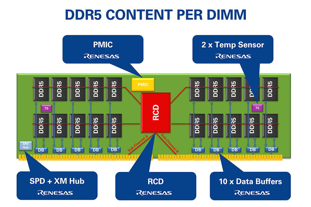
Fast forward, and our newest DDR5 memory interfaces include second-generation RCDs and data buffers for MRDIMMs in addition to a power management IC (PMIC), making us the only company to offer a complete chipset solution for the next-generation of RDIMMs and MRDIMMs. In addition, Renesas has made a significant contribution in helping power efficiency by evangelizing a concept called "voltage regulation on DIMM." Voltage regulation circuitry now sits directly on the DIMM, as opposed to the motherboard, which allows for a more efficient, distributed power model. This is done using PMICs that locally generate and regulate all the necessary voltages needed by various DIMM components.
Leveraging the Electronics Design Ecosystem for the Future
Renesas has amassed a vast base of in-house expertise by collaborating with a large design ecosystem of leading CPU and memory providers, hyperscale data center customers, and standards bodies like JEDEC. That gives us the freedom to remove the bottlenecks that stand in the way of our ability to continue increasing DIMM speeds and capacity by determining how many DRAM components can be populated and how fast they can run.
It also opens opportunities to leverage technologies developed for AI data centers and redirect them to emerging use cases. That's true for the higher processing and memory bandwidth requirements influencing designs at the edge of industrial network controls, where data must be captured and turned into actionable insights. And, it applies to the surging data volumes required by automotive safety and autonomous driving applications, which are quickly turning our vehicles into servers on wheels.
If there's one thing we've learned in our efforts to align our memory interface technology with the demands of the AI age, it's that data hates to rest. It's always moving. So are we.