
There are two major applications for FemtoClock™ 3 Wireless (3W): One is wireline for 224G PAM SerDes reference clocks, and the other is wireless for "5G Advanced" radio units or small cell.
Due to GPU farm/AI node ramping in recent days, all the networking speeds are moving from 112G PAM4 to 224G PAM4 SerDes (from 800G to 1.6T) for Gen AI. Multiple Ethernet switch vendors – Broadcom, Nvidia, Marvell, and Cisco will have Ethernet switch chipset solutions in the market shortly, and the ultra-low jitter clock solution becomes essential for them. FemtoClock 3W (RC38312A) is targeted for this application.
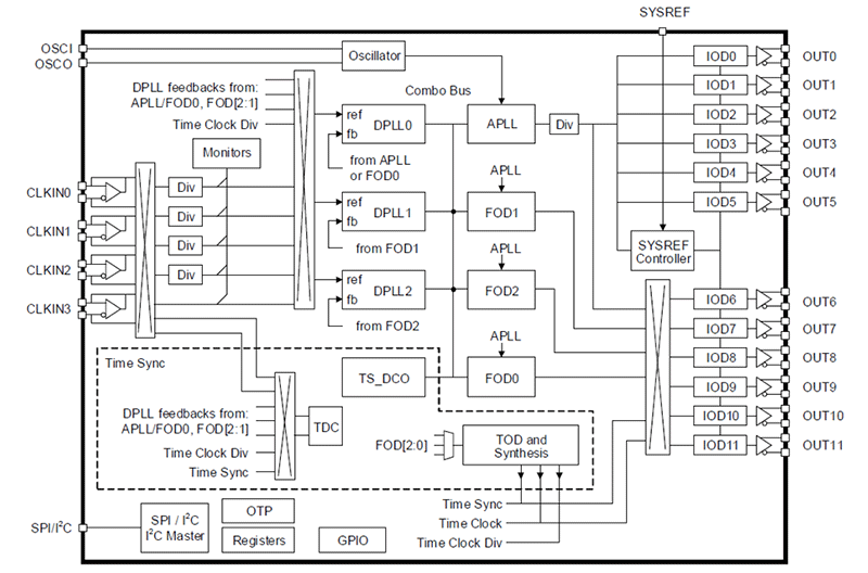
RC38312A Features
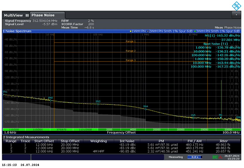
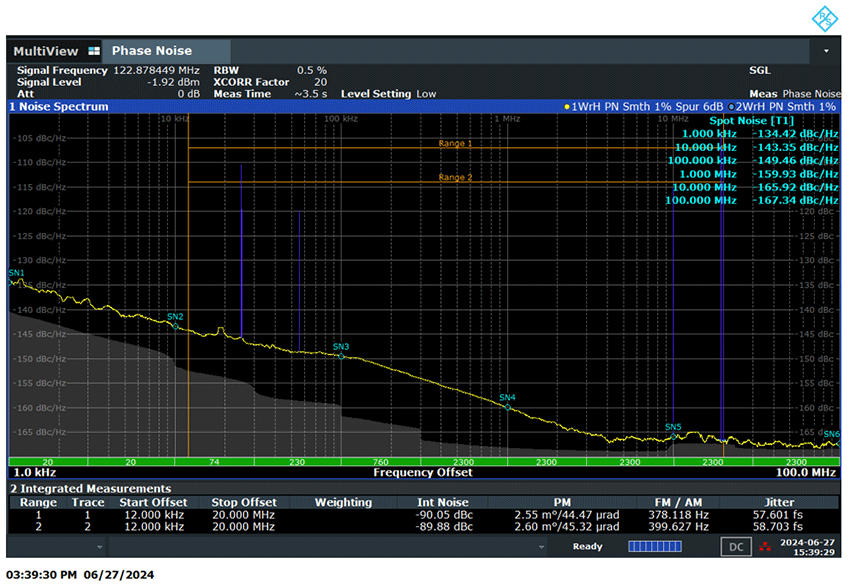
- Ultra-low phase noise synthesizer with jitter below 25fs RMS, 12kHz to 20MHz with 4MHz HPF
- 3 DPLL and 3 FOD to support 4 frequency domains
- Support for JESD204B/C
- 12 clock outputs with independent integer dividers:
- 8: LVDS, HCSL (AC-LVPECL) or CML
- 4: LVDS, HCSL (AC-LVPECL) or LVCMOS
- Output frequency range:
- CML: DC to 2.5GHz
- LVDS or HCSL: DC to 1GHz
- LVCMOS: DC to 250MHz
- Four differential or eight single-ended clock inputs
- Can operate with a single 1.8V supply
- Power consumption is less than 1.5W
Clock Requirements for 224G PAM4 SerDes
The clock requirements for 224G PAM4 SerDes are stringent and FemtoClock 3W can meet them. The jitter requirements for 224G PAM4 are below 25fs (12kHz to 20MHz) with 4MHz HPF and FemtoClock 3W meets the requirements within margin.
Support for Both Wireline and Wireless Timing
RF frequency synthesizers are essential components in the advanced modern communication software-defined radio system. The spectral purity of these synthesizers is critical, as it directly impacts the maximum achievable data rate and noise-power characteristics. In RF applications, synthesizers must deliver high frequencies with a broad tuning range and precise frequency resolution. Achieving these demanding performance standards requires not only limited power consumption and compact chip area but also minimal spurious tones and phase noise.
In real 1024-QAM applications, you can understand the jitter impact to the diagram. The protocol still helps to reduce the error. In commercial SDR communications systems, the best clock jitter performance is the key strategy to win the business for top-tier customers. It impacts the transmission distance and data rate.
Advanced Architecture
In 4G radio design, the PLL system was using external VCXO to provide the low jitter clock solution and JESD204B/C was designed by PLL and FPGA. Complexity and cost are the key issues to trigger innovation, and synchronization was using another DPLL. It makes the timing system come with Synch DPLL, FPGA, and a dual loop jitter attenuator with external VCXO, 4 components in total.
In the modern radio design, FemtoClock 3W has had improvements including a single chip supporting low phase noise PLL, 3 DPLL, 3 Fractional Output Dividers (FOD), combo bus, SYSREF/JESD204B/C engine, and TimeSync Module for Sync application.
Ultra-Low Phase Noise for Radio Applications
As mentioned earlier, the phase noise is critical for mmWave radio applications. FemtoClock 3W is designed based on the BGA package (low crosstalk), low phase noise PLL (Kronos PLL), CML output to 2.5GHz (high-frequency output channel), phase adjustment, and compensation.
3GPP Timeline
Rel-19 content was decided at the December 2023 TSGs (#102), and it is critical for customers that define "5G-Advanced”.
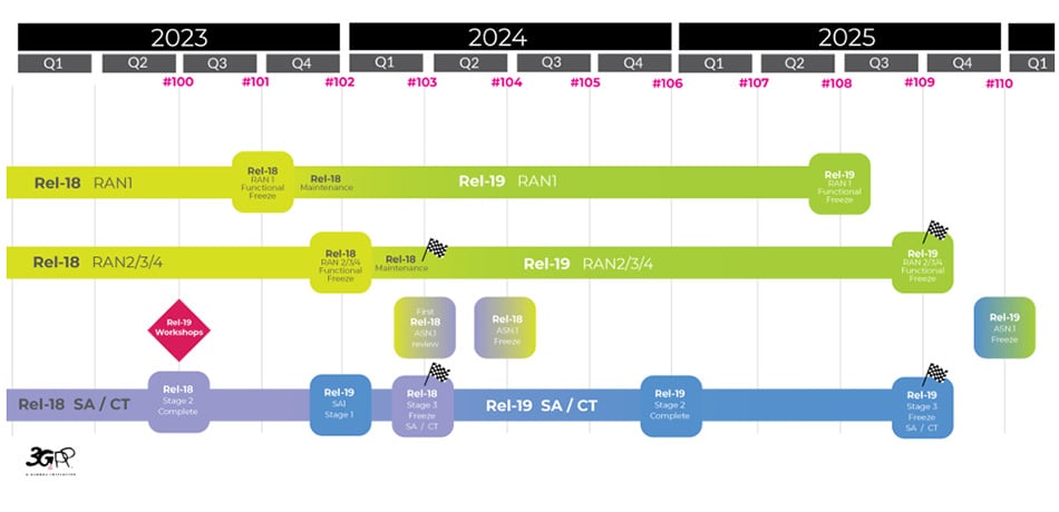
Source: https://www.3gpp.org/specifications-technologies/releases/release-19
Conclusion
FemtoClock 3W is Renesas' latest PLL technology, supporting both wireless and wireline applications. With a single 1.8V power supply, it offers the lowest power consumption and the ultra-low phase jitter clock output.
FemtoClock 3W is the best clock solution for both wireless radio units and 224G PAM4 SerDes reference clocks for 1.6T Ethernet switches.
To begin evaluating FemtoClock 3W, get an evaluation kit today!
