
Features
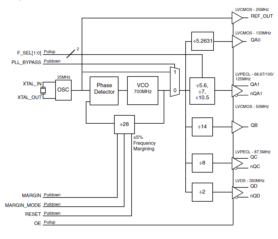
- 5 banks of outputs:
One single-ended LVCMOS reference clock output at: 25MHz
Bank A: one single-ended (QA0) LVCMOS output at: 133MHz and one (QA1/nQA1) LVPECL output at: 66.67MHz, 100MHz and 125MHz
Bank B: one (QB) LVCMOS output at: 50MHz
Bank C: one (QC/nQC) differential LVPECL output at: 87.5MHz
Bank D: one (QD/nQD) differential LVDS output at: 350MHz - Crystal input frequency: 25MHz
- ±5% frequency margining
- Full 3.3V operating supply
- 0°C to 70°C ambient operating temperature(refer to Table 7 on page 11)
- Available in lead-free (RoHS 6) package
- For replacement part use 8T49N282B-dddNLGI
Description
The 843S2807 provides five banks of outputs and a reference clock. The banks can be enabled by using a common output enable pin. A 25MHz crystal is used to generate the 50MHz, 66.67MHz, 87.5MHz, 100MHz, 125MHz, 133MHz and 350MHz frequencies.