Overview
Description
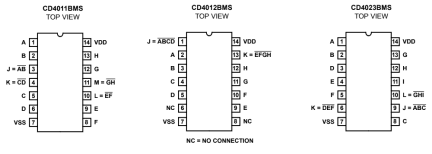
The CD4023BMS is a triple 3-input CMOS NAND gate that provides the system designer with direct implementation of the NAND function and supplements the existing family of CMOS gates. All inputs and outputs are buffered. The CD4023BMS is supplied in these 14-lead outline packages: Braze Seal DIP H4Q, Frit Seal DIP H1B and a Ceramic Flatpack H3W.
Features
- High-voltage types (20V rating)
- Propagation delay time = 60ns (typ.) at CL = 50pF, VDD = 10V
- Buffered inputs and outputs
- Standardized symmetrical output characteristics
- Maximum input current of 1µA at 18V over full package temperature range; 100nA at 18V and +25 °C
- 100% tested for maximum quiescent current at 20V
- 5V, 10V and 15V parametric ratings
- Noise margin (over full package temperature range):
- 1V at VDD = 5V
- 2V at VDD = 10V
- 2.5V at VDD = 15V
- Meets all requirements of JEDEC tentative standards No. 13B, "Standard Specifications for Description of "B" Series CMOS devices
Comparison
Applications
Design & Development
Models
ECAD Models
Schematic symbols, PCB footprints, and 3D CAD models from SamacSys can be found by clicking on products in the Product Options table. If a symbol or model isn't available, it can be requested directly from the website.


