About This Video
Transcript
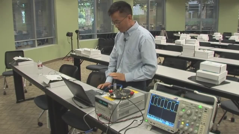
Hi, my name is Shudong Zhen. I'm the application engineer in IDT timing group. Today, I'm going to introduce you to the VersaClock 5 Evaluation Board. The board comes in a box, a full package. First of all, of course, this board is out of the static bag.
This is the board with the USB cable. So, this is the board. It has two power systems. As you can see, there are two red banana jacks and one black banana jack for the power return. Also, we support the USB power for the whole board.
For this demonstration, I'm going to use the USB power because this is the first power supply we recommend you to use. It's easy. You don't need to connect the cables to the bench power supply.
Now here, we have the VersaClock 5 timing commander GUI opened up in a computer and right now, the board is not connected to the software. So, you can see there's no sign of communication between the software and the board. Now, let's make a connection to the board. The USB cable that comes with the box and one side, plug into the USB connector of the PC and then the other side goes to the board, the mini USB connector.
Now, up until this point, we're still not seeing the connection because we need to click on this chips symbol sign to make the connection but before I do that, I want to show you the default frequency output from the board.
Now, here is the scope, with the SMA connector cables. I'm going to connect these to the output one of the board. As you can see, on the scope screen, there is already 100 MHz LVCMOS differential output already, as you can see. So, this is the default output from the chip, output one and one B. As you can see, if I disconnect the power, there's no output and then when I connect to the power, the output is coming out right away. That's the default output.
Now, on this very same output, if I, in the VersaClock 5 Timing Commander GUI, if I change that output to 125 MHz, you're going to see the frequency change. Right now, this is the point I need to make the connection to the board so that the configuration can be downloaded into the chip.
So, first of all, click on the chip sign and then, as you can see, this area becomes green, which is a sign of successful connection to the board. Now, on the right side of this sign, if you hover the mouse onto the sign, you can see write all registers to the chip. Right now, I have 25 megaHertz crystal input. I entered 25 into the input frequency box and then, on the output frequency box for output one, I have entered 125 MHz.
Now, once I write this configuration into the chip, you're going to see the change on the screen, on the scope screen. Now, the GUI shows WriteAll has completed. The scope screen should have shown the 125 MHz output from the default 100 MHz. So, the configuration of the board is very easy once we have a good connection. The desired output frequency can be immediately displayed.
We can also use the bench power supply to power the board. These two red banana jacks and the one black banana jack are for the bench power supply. If we use this cable from the bench power supply to make the connection... So, this is a green cable but still, we use it as a power supply, 3.3 volts and this is for the return, the power return. At the same time, the USB cable can still be connected for the data communication. The power supply is provided by the connectors, although we need to make the jumpers. We know the jumpers will make the selections between the USB power and the jack power. In this case, for example, as you can see, the labels on this connector, the VDDD_J means the power is coming from the jack. So, we need to move the connector into the left side and it's the same move for all the other jumpers, to make the power supply switch. That's for the power supply and then I think that concludes the introduction to the VersaClock 5 Evaluation Board. Thank you very much for you time to listen to this video. Thank you.
