Overview
Description
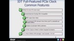
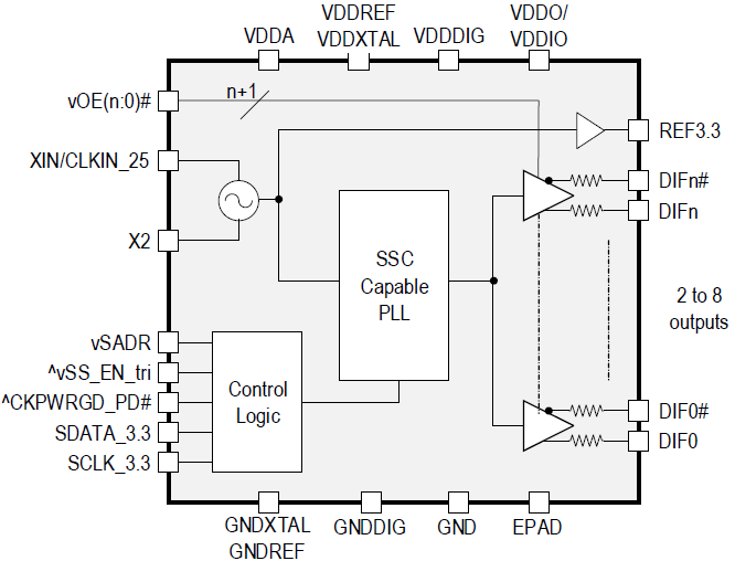
The 9FGL0241/51 devices are 2-output 3.3V PCIe Gen 1–6 clock generators. Each output has a dedicated OE# pin supporting PCIe CLKREQ# functionality. Two different spread spectrum levels, in addition to spread off, are supported. The 9FGL0241/51 supports PCIe Gen 1–6 Common Clocked architectures (CC), PCIe Separate Reference no Spread (SRNS), and Separate Reference Independent Spread (SRIS) clocking architectures.
Features
- PCIe Gen 1–6 CC-compliant
- Supports PCIe SRIS and SRNS clocking
- Integrated terminations for 100Ω and 85Ω systems save 4 resistors per output
- Pin-selectable SRNS 0%, CC 0%, and CC/SRIS -0.5% spread
- SMBus-selectable CC/SRIS -0.25% spread
- One 3.3V LVCMOS REF output with Wake-On-LAN (WOL) support
- Easy AC coupling to other logic families, see application note AN-891.
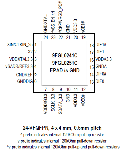
- Space saving 4mm × 4mm 24-VFQFPN
Comparison
Applications
- Servers/High-Performance Computing
- nVME Storage
- Networking
- Accelerators
- Industrial Control
Design & Development
Models
ECAD Models
Schematic symbols, PCB footprints, and 3D CAD models from SamacSys can be found by clicking on products in the Product Options table. If a symbol or model isn't available, it can be requested directly from the website.

Processing table
Pkg. Type |
Lead Count (#) |
Temp. Grade |
Output Impedance |
Carrier Type |
Moisture Sensitivity Level (MSL) |
Price (USD) | 1ku |
Buy / Sample |
|
|---|---|---|---|---|---|---|---|---|
| Part Number | ||||||||
| VFQFPN | 24 | I | 100 | Tray | 1 | 2.563 | Get Samples, | |
| VFQFPN | 24 | I | 100 | Reel | 1 | |||
| VFQFPN | 24 | I | 85 | Tray | 1 | Get Samples, | ||
| VFQFPN | 24 | I | 85 | Reel | 1 |
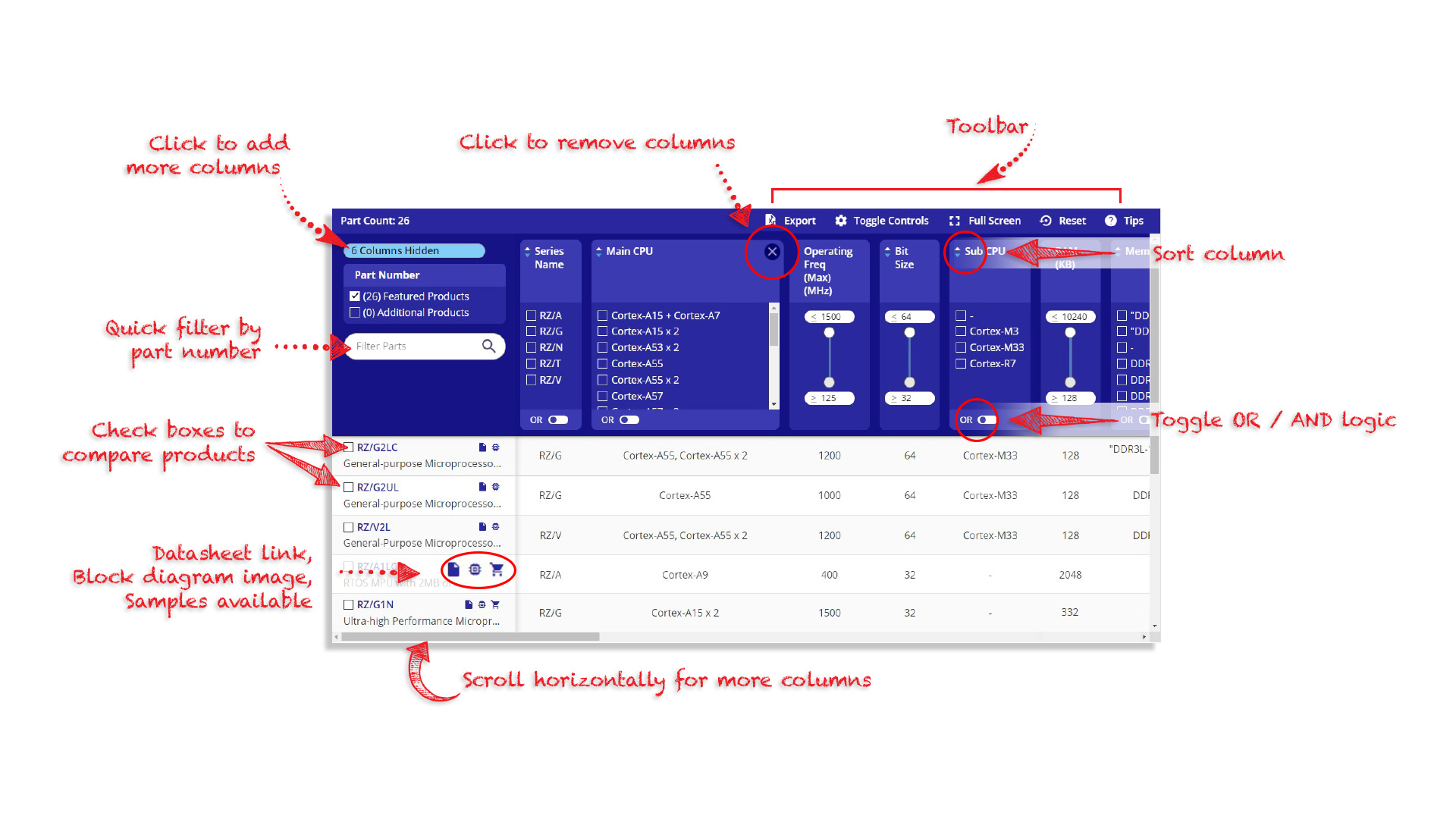
Tips for Using This Parametric Table:
- Hide Filters button in header: Collapse or expands filters
- Column sort buttons in header: Sort Column alphabetically / numerically descending or ascending
- Reset button in header: Reset all filters to the page default
- Full Screen button in header: Expand the table to full screen view (user must close out of full screen before they can interact with rest of page)
- Export button in header: Export the filtered results of the table to an Excel document
- Filter parts search bar in header: Type to filter table results by part number
- Hide column button in column headers: Select to hide columns in table
- AND / OR toggle switches in header: Toggles the logic of this particular filter to be “AND” or “OR” logic for filtering results
- Multiselect checkboxes at beginning of each row in table: Select these checkboxes to compare products against each other
- Document icon next to product name in row: View the featured document for this product
- Chip icon next to the right of the document icon in row: View the block diagram for this product
- Cart icon to the right of the chip icon: Indicates that samples are available for this product
Videos & Training
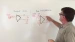
PCIe Reference Clock Jitter Budgets
Ron Wade, chief PCIe system architect explains the fundamental difference in reference clock jitter budgets between the first three generations of the specification and those of Gen4 and Gen5 which raise new challenges for designers.
Related Resources
Video List