Absolute Maximum Ratings
Isolation Voltage: BV (Vrms)
The allowable maximum alternating current voltage that can be applied between the input pins and output pins is expressed as a root mean square (rms) value. This value guarantees a certain insulation resistance. Normally, this value is guaranteed not for an unlimited period, but for a limited test time, of 1 minute, for example.
Operating Ambient Temperature: TA (°C)
The allowable temperature range in which power application is possible. Usually when the ambient temperature rises, the power dissipation (PD, PC) declines. Moreover, power application is inhibited when the actual ambient temperature is out of this range. In the case of photocouplers, the temperature at which power can be applied is not described as the "package surface temperature", but instead as the "ambient temperature (air temperature around the device)".
Storage Temperature: Tstg (°C)
The allowable temperature range when power is not applied (stored state).
Light-Emitting Diode (LED): Forward Current: IF (mA)
The allowable maximum current at which destruction does not occur, within the allowable power dissipation (PD) range of the LED on the light-emitting side when the ambient temperature is 25 °C.
Light-Emitting Diode (LED): Reverse Voltage: VR (V)
Note that the reverse withstand voltage of the LED on the light-emitting side is low. When the reverse withstand voltage is exceeded, a reverse current suddenly flows. In this case, the LED does not emit light. Additionally, when a reverse current flows, the subsequent light-emitting efficiency is lowered. Therefore, when a reverse voltage exceeding this value is applied even momentarily, destruction or non-recoverable degradation may occur. However, in the case of AC (alternating current) input type photocouplers, there is no such value since both the positive and negative voltages are forward voltages.
Light-Emitting Diode: Power Dissipation: PD (mW)
The allowable power dissipation of an LED on the light-emitting side at an ambient temperature of 25 °C. Generally, allowable power dissipation (PD) tends to decline as the ambient temperature rises, as shown in the following figure.
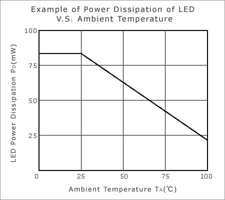
The allowable power dissipation is obtained for the actual maximum ambient temperature from the above "PD-TA" curve. In addition to the absolute maximum rating of the "Light-Emitting Diode: Forward Current (IF)", when a forward current (IF) that exceeds the value obtained by dividing this allowable power dissipation by the forward voltage (VF) flows, destruction or non-recoverable degradation may occur.
Phototransistor: Power Dissipation: PC (mW)
The allowable power dissipation of a light-receiving phototransistor when the ambient temperature is 25 °C. Generally, the allowable power dissipation (PC) tends to decline as the ambient temperature rises, as shown in the following figure.
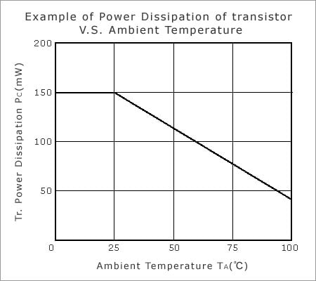
The power dissipation is obtained for the actual maximum ambient temperature from the above "PC-TA" curve. In addition to the absolute maximum rating for the "Phototransistor: Collector Current (IC)", when a collector current (IC) that exceeds the value obtained by dividing this value by the collector-to-emitter voltage (VCE), destruction or non-recoverable degradation may occur.
Phototransistor: Collector-to-Emitter Voltage: VCEO (V)
The allowable maximum voltage that can be applied between collector and emitter of a phototransistor on the light-receiving side when no forward current flows through the LED on the light-emitting side (when the LED does not emit light). Generally, when the power supply voltage approaches this value, the transient operation locus cannot be kept within the allowable power dissipation range for the actual maximum ambient temperature during switching, and destruction by excess power loss may occur in the moment of switching operation. Note this and keep the power supply voltage within a sufficient safe range so that excess power loss does not occur even in such transient time.
Phototransistor: Emitter-to-Collector Voltage: VECO (V)
The allowable reverse voltage that can be applied to a phototransistor on the light-receiving side. Generally, this voltage depends on the reverse withstand voltage between the emitter and base of the phototransistor and is low. If a reverse voltage that exceeds this value even momentarily is applied, destruction or non-recoverable degradation may occur.
Phototransistor: Collector Current: IC (mA)
The allowable maximum collector current that can flow through a phototransistor within the allowable power dissipation (PC) range when the light-receiving phototransistor is conducting current at an ambient temperature of 25 °C.
Electrical Characteristics
Current Transfer Ratio: CTR (%)
The value that expresses the collector current (IC) ratio in relation to a prescribed forward current (IF), when a given collector-to-emitter voltage (VCE) is applied to the light-receiving phototransistor.
CTR (%) = 100 x IC/IF
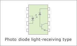
Even in the photo diode light-receiving type shown in the following figure, this value is defined as the collector current (IC) ratio in relation to a prescribed forward current (IF) flow through the light-emitting diode.
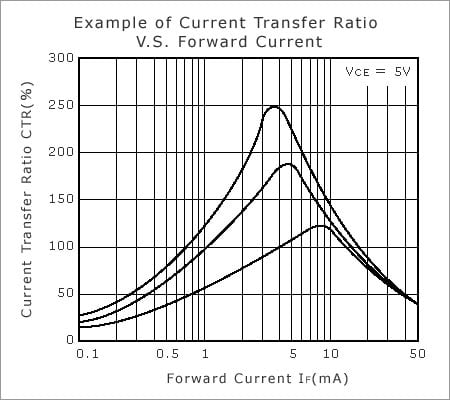
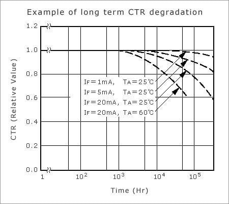
Generally, CTR varies according to the forward current (IF), ambient temperature (TA) or the collector-to-emitter voltage (VCE) in actual. It also changes over time according to the actual ambient temperature (TA) and forward current (IF) during use. When actually using a photocoupler, obtain the minimum forward current (IF) value required for conducting the prescribed collector current (IC) into the light-receiving phototransistor, for the ambient temperature (TA), collector-to-emitter voltage (VCE) and total operating time, using the CTR-IF curve, CTR-TA curve, VCE-IC curve, and long-term CTR degradation curve, and design the forward current (IF) value equal to or greater to that minimum value.

Isolation Resistance: RI-O (Ω)
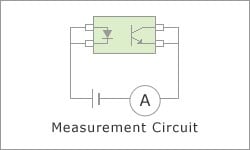
The initial isolation resistance when a high direct-current voltage is applied between the input and output pins. Since the isolation resistance may decline depending on the usage environment, such as for humidity, or the application time of the voltage, take actual usage conditions into consideration when designing and testing devices.
Isolation Capacitance: CI-O (pF)
The capacitance when a high-frequency signal is applied between the input and output pins. A sudden change of the electric potential difference between the input pin and output pin may cause noise in the output through this capacitance. Therefore, some products prescribe the immunity to such transient as specification of "common mode transient immunity (CMTI)". Since this value may increase depending on the wiring conditions, etc., take these factors into consideration when designing and testing devices and during actual use.

Common Mode Transient Immunity: CM (kV/µs)
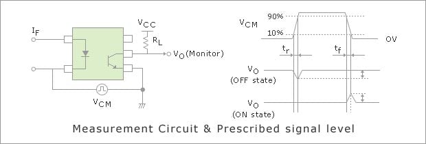
When a sudden change of pulse is applied between the input and output pins while a load resistor is connected to the output phototransistor and a power source is applied, some noise may be caused in the collector-to-emitter voltage of the output phototransistor. This is defined as the pulse's rising/falling speed.
Light-Emitting Diode: Forward Voltage: VF (V)
The inter-pin voltage when a forward current flows through an LED on the light-emitting side. The product of this value and the forward current value expresses the internal loss of the light-emitting side. Generally, the increasing of the forward current or the falling of the ambient temperature causes rising of the VF voltage.
Light-Emitting Diode: Reverse Current: IR (µA)
This current flows when a prescribed reverse voltage is applied within the maximum rating range to the LED on the light-emitting side. Generally, the increasing of the reverse voltage or the rising of the ambient temperature causes this current to increase. In the case of circuits in which a reverse voltage is applied to the LED, design the drive circuit taking into consideration that this value is affected by usage conditions.
Light-Emitting Diode: Terminal Capacitance: Ct (pF)
The capacitance between LED pins on the light-emitting side. Mainly when a photocoupler is turned off, if the electric charge accumulated in this capacitance is not quickly discharged, a small current is continuously discharged through the LED and as a result turning off of the output is delayed. If the drive circuit features a switch in parallel with the LED, as shown in the left figure below, when the LED is turned off, there is no problem since the electric charge is quickly discharged via this switch. On the other hand, if the switch is placed in series with the LED as shown in the right figure, faster turn-off characteristics can be obtained by placing a discharge resistor in parallel with the LED.
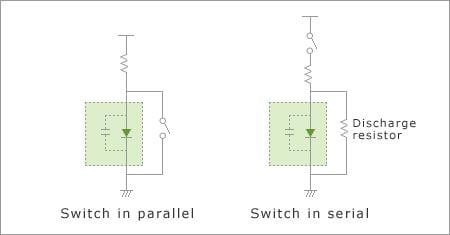
If the LED is driven by logic gate, a switch is provided both in series and in parallel. Therefore, basically discharge occurs quickly. However in the case of a logic gate with a low drive capability, or gate with high saturation output voltage, it may be necessary to provide a discharge resistor in parallel.
Phototransistor: Collector-to-Emitter Dark Current: ICEO (nA)
The leakage current of the collector of the phototransistor on the light-receiving side, when no forward current flows through the LED on the light-emitting side (in which case the LED does not emit light). Generally, increasing the power supply voltage or raising the ambient temperature causes this current to increase. Regarding the value of the load resistor, take the maximum value of this current within the usage condition ranges into consideration when designing devices.
Phototransistor: Collector Saturation Voltage: VCE(sat) (V)
The collector-to-emitter voltage in relation to a prescribed collector current (IC) of the phototransistor on the light-receiving side, when a prescribed forward current (IF) flows through the LED on the light-emitting side. Since this voltage changes greatly depending on the forward current (IF), collector current (IC), and individual variations in the current transfer ratio (CTR) and its degradation, the forward current and collector current values must be designed taking these factors into careful consideration.
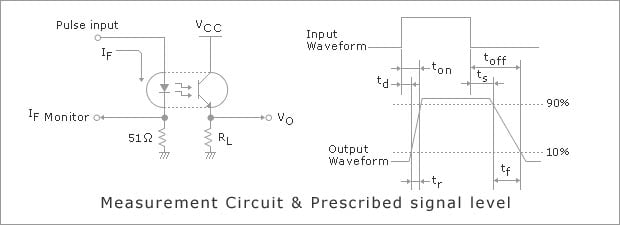
Rise Time/Fall Time: tr, tf (µs)
The transient change time of the output voltage when the output is switched ON/OFF while a forward current (IF) flows through an LED on the light-emitting side as a pulse. The inverse number of the sum of these two values is almost proportional to the maximum operating frequency for the drive conditions.
Propagation Delay Time: tP (µs)
The delay time from forward current change to output voltage change, when a forward current (IF) flows through an LED on the light-emitting side as a pulse. It resembles "Rise Time/Fall Time", but the definitions are different. The "Propagation Delay Time" means the time from input change to output change. When the angle for the drive signal cycle is defined as 360 degree(2π radians), the angle value corresponding to this value is almost equal to the signal phase delay.
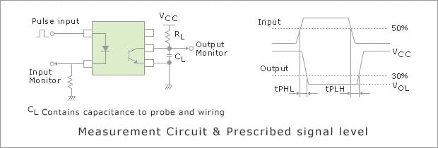
The mechanism by which the propagation delay time is generated is the same as that for usual transistors, but in the case of photocouplers, it is basically not possible to temporarily convert the base potential into a reverse bias to reduce the delay at turn-off as can be done for usual transistors. Basically, you should select a product based on sufficient operation speed. However, if the occurrence of slow operation products due to variation is a possibility, this may be improved by limiting ranking in the case of products with a current transfer ratio (CTR) ranking.