The increasing popularity of the RISC-V ISA within the semiconductor industry is a boon for innovation. It provides designers with unprecedented flexibility and will slowly but steadily challenge and transform the current landscape of embedded systems. In the past, Renesas has embraced RISC-V technology introducing 32-bit ASSP devices for voice control and motor control built on CPU cores developed by Andes Technology Corp.
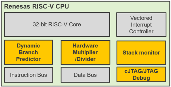
The exciting next step is the availability of the first, in-house engineered, CPU core. A high-level block diagram of the CPU is shown below:

But what‘s so special about it? First, this CPU is suitable for many different application contexts. It can be used as the main CPU or to manage an on-chip subsystem or even to be embedded in a specialized ASSP device. Clearly, it is very flexible. Second, the implementation is very efficient in terms of silicon area, which helps reduce operating current and leakage current during standby time, besides the obvious effect of a smaller cost impact. Third, despite targeting small embedded systems, it provides a surprisingly high level of computational throughput to fulfill the increasingly demanding performance requirement of even deeply embedded applications.
At its base, the implementer can choose between the RV32 ‘I’ or ‘E’ option to optimize the available number of general-purpose registers. For example, in the case of a small subsystem that does not need to process complex stacks and applications but is dedicated to servicing a specific peripheral or doing housekeeping tasks.
The RISC-V ISA also foresees several ‘extensions’ that target specific functionality in a better or more efficient way than it can be done using the standard mandatory ISA. Renesas chose to integrate several of those:
- M extension – speeds up and optimizes multiplication (and division) operations, leveraging a hardware multiplier and divider unit for fastest instruction execution
- A extension – supports atomic access instructions, useful as a foundation for concurrency and exclusive access management typically in RTOS-based systems
- C extension – defines compressed instructions which are encoded in 16-bits only and are particularly interesting because they can easily save memory space for common and frequent instructions allowing the compiler to select those optimizations where possible; a simple trick that can shrink the code and improve performance at the same time
- B extension – adds several instructions for bit manipulation, a bit advantage for applications managing peripheral registers, protocols, and data structures based on bit field encoded values where the functionality of a composed set of generic instructions can often be replaced by a single dedicated one
This is the beauty of the RISC-V ISA concept, built from the ground up to allow the designer to choose which elements to include in the processor, dependent on their target use case, and as a result optimize the trade-off between the resulting power consumption, performance, and silicon footprint. Engineering-wise, it is a very elegant way to make sure you “pay the price” only for those things you really want to implement.
To enhance the robustness of the application software, a stack monitor register is added. This is very useful to detect and prevent stack memory overflows, which are quite common issues but sometimes hard to spot through test coverage alone. As those problems may compromise the integrity of the system and generate application misbehavior at runtime, it is quite a nice feature to have and a fundamental safety net for controlling such unforeseen events.
Even the simplest control system typically must manage several decision paths to service the application and call the appropriate processing routines at any time. Or repeatedly perform some repeated computations on data buffers. Therefore, the implemented code will have several branches, loops, and decision points where the program flow might change depending on the context. As such a pattern is common, the CPU also features a dynamic branch prediction unit to make such processing more efficient. The role of the branch predictor is to observe the code behavior and then dynamically infer the next instruction most likely to be executed during such control loops. If we assume it will do a good job in that, it will sensibly improve the average code execution throughput by making the right guess when choosing the next instruction to fetch for execution.
The next building block to call out relates to debug capabilities. Besides the standard JTAG, the CPU also supports the two-wire compact JTAG debug interface, which is very suitable for the smallest microcontroller packages where the amount of user application pins can be limited. Several performance monitor registers are also implemented in the CPU, which allows benchmarking the runtime behavior of the executed code in an easy way.
Another key factor of any embedded system is the responsiveness to events, and in the deeply embedded devices at microcontroller levels hard real-time behavior is mandated, meaning the application has a bounded amount of time to respond to a certain event. A low response latency can have many different benefits: allow the application to service more concurrent events, provide a reasonable time margin to ensure proper task handling, or maybe throttle the CPU speed for additional power savings. At an architectural level, the Renesas implementation adds a register bank save function to improve the latency and enable the developer to enjoy its benefits. It is possible to backup and restore the CPU working registers and speed up context switching, in the case of interrupt servicing, or when an embedded RTOS must swap out the currently executed thread in response to an event, to cite two almost immediate examples.
To further assist developers in benchmarking an application and verifying its behavior, an efficient and compact instruction tracing unit is also available which provides further insight into the runtime behavior of the system.
This outlines details about the CPU features, some of which can be selected depending on the application and market requirements. But what else should be considered to evaluate and make a real product based on such new technology? First is that required toolchains are available as part of the necessary infrastructure to develop and deploy a solution. Customers will be able to benefit from either the Renesas e2 studio environment with its configuration plugins or any major commercial third-party IDE supporting RISC-V based MCUs. These are all ready to use.
Second is that the CPU implementation is not just simulated, its features have been designed and validated in a real silicon product implementation. Initial benchmarks showed an impressive 3.27 CoreMark/MHz performance while using an open source LLVM-based compiler toolchain, outperforming comparable architectures available on the market. Further details about this excellent score will be found on the EEMBC website once the first product is unveiled in early 2024. As many will note, the performance of a proprietary commercial compiler, once verified, is reasonably expected to be even higher than preliminary results.
This new CPU is a keystone for the next steps, creating an additional and complementary option in the existing Renesas MCU portfolio. Renesas is ready to support customers with the broadest range of solutions with the inclusion of the innovative and growing RISC-V architecture.
Be sure to stay tuned at renesas.com/risc-v to find out more soon.

