Electronics design engineers want it all: programmability, low power, low cost, small footprint, fast time-to-market, and a quick and easy product configurability process – without learning new software. At Renesas, that's exactly the need we address with our GreenPAK™ line of configurable ICs and the ForgeFPGA™ family of low-density programmable logic.
Created by Silego, which Renesas obtained through our strategic acquisition of Dialog Semiconductor, GreenPAK "silicon Legos" are mixed-signal devices defined by analog and digital building blocks and one-time-programmable, non-volatile memory. For customers resigned to spending weeks or months on an expensive and onerous design process, GreenPAK's build-as-you-go approach to configurable silicon allows them to create a custom ASIC on their desktop in a matter of hours.
Renesas' user-friendly software tool environment, known as the Go Configure™ Software Hub, supports the entire GreenPAK configurable mixed-signal portfolio as well as the low-power line-up of ForgeFPGA devices. Both product families benefit from a graphical user interface (GUI) that requires no particular programming language fluency.

GreenPAK: Where Programmability Meets Accessibility
The growing programmable mixed-signal GreenPAK portfolio features several thousand custom products birthed from about 50 different base die. Each die includes a variety of macrocells, lookup tables, counters, delays, flip-flops and latches, op amps, and built-in analog-to-digital and digital-to-analog converters for signal and voltage-reference monitoring. Renesas also offers an Asynchronous State Machine (ASM) macrocell, which allows users to quickly develop their own custom state machines.
GreenPAK shrinks part count and board space requirements and lowers power consumption by integrating 10 to 30 components into a single custom IC, which can reduce bill of materials costs by up to three times. In addition to accelerating time-to-market, GreenPAK devices eliminate the costly Non-recurring Engineer (NRE) charges of custom ASICs.
In the interest of accessibility, GreenPAK design software enables the customer to either work fully autonomously, shield some proprietary aspects of their design, or provide a rough schematic that our global applications engineering team will use to create their design. To that end, customers can download the Renesas GreenPAK Cookbook, a guide to configurable, mixed-signal design techniques and applications for GreenPAK ICs that offers system-level circuit designers cost-effective, personalized solutions.
Once the design is complete, the GreenPAK GUI outputs a uniquely secure configuration file that is burned onto non-volatile memory. If the design changes, the engineer can re-spin a new device in a matter of minutes.
How have customers responded? To date, we've shipped more than five billion GreenPAK devices across consumer, industrial, communications, and AEC-Q100-certified automotive applications ranging from supervisory circuits, system reset, and power sequencing to motor and temperature controls.
In one instance, a customer created a simple power line communication protocol between a True Wireless Stereo (TWS) earbud and the charging case. In another, one of our newest GreenPAK devices replaced a highly integrated incumbent boost converter used for driving a buzzer motor to meet the customer's ambition to miniaturize their design by at least 30 percent through a 50 percent reduction in board size and power consumption. Customers repeatedly amaze us by using GreenPAK in ways we never imagined.
Augmenting GreenPAK with the Renesas ForgeFPGA Family
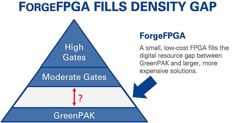
Complementing the GreenPAK suite, Renesas is also expanding our ForgeFPGA family to target a deeply underserved corner of the market – low-cost field-programmable logic. Whereas other FPGA device providers are locked in a density race that has yielded tens of millions of logic gates per device, many designers confined by modest cost and power budgets may only require a thousand or more lookup tables. The difference between the two is stark: high-density FPGAs can easily cost upwards of $1,000, while ForgeFPGA processors are available in volume for less than 50 cents.

Renesas' low-density ForgeFPGA processors are designed specifically for the kinds of low-cost applications that previously would have used a high-cost FPGA or some combination of an MCU and external circuitry. Use cases include high-volume consumer and IoT applications such as data pipelining, protocol conversions, and sensor interfacing.
ForgeFPGA software is available with two development modes: a macro-cell that uses a schematic capture-based development flow and an HDL mode that provides a familiar Verilog environment for experienced FPGA developers. Users can freely switch between the modes on the fly.
Whether working with GreenPAK ICs or ForgeFPGA processors, customers constrained by power, space, and cost now have access to two complementary programmable device models. Both are distinguished by easy-to-use software, free licenses, and worldwide application support that helps them increase speed and efficiency for cost-sensitive designs.
