In our previous blog about the importance of analog-to-digital converters (ADCs), we focused on the various architectures that are in common usage for the Industrial Internet of Things. In particular, we looked at which architecture was best for low-latency, low-power and high-precision applications, with each option having various advantages and disadvantages. When we looked at the applications requiring low latency and low power consumption, the successive approximation register (SAR) ADC provided the best overall solution versus other architectures such as flash, delta-sigma and pipeline.
The ADC choice is a bit different for the increasing number of applications which require faster sampling rates to meet the growing demands of machine-to-machine (M2M) connections. In a recent article, we discuss how these connections are increasing dramatically with the growth of the internet of things, and the ADC, which resides in the analog front end (AFE), is central to these connections. So, what are the trade-offs that need to be considered and which architecture shines above the others for applications requiring fast sampling rates?
Consider again the SAR ADC. In this architecture, the analog input signal is sampled, and is then compared to successive reference voltages by a single comparator working at a higher frequency than the sampling rate.

Figure 1. SAR ADC Block Diagram
Within one sampling period, the comparator needs to make at least as many decisions as the converter resolution. A higher resolution reduces the maximum sampling rate, which is dependent on how quickly the comparator can make a decision and how fast the SAR logic can run. In a switched capacitor implementation, the ADC input network equivalent circuit, as shown in figure 2, basically comprises a sampling capacitor and a sampling switch.

Figure 2. SAR ADC Input Network
The sample and hold (S&H) operation is embedded in the DAC circuitry, and the sampling capacitor is sized to meet the noise requirements. With this configuration and correct sizing of the sampling capacitor, the SAR ADC can convert very high frequency signals (tens of MHz) without resulting in high power dissipation.
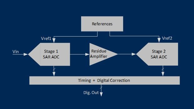
A second architecture to consider is the SAR-assisted pipeline ADC, shown in figure 3. This ADC IP can be implemented with two lower-resolution SAR ADC stages and a residue amplifier. The first stage resolves the most significant bits of the digital output word. The residue is amplified and sampled by the second stage. As each stage is using a lower resolution, a fast conversion time per stage is achievable. Both stages work simultaneously; while stage two is converting the residue amplified signal, stage one is already sampling and converting the next sample. This pipelining allows for a considerable increase in the maximum sampling rate versus a single SAR architecture.

Figure 3. SAR-Assisted Pipeline ADC Block Diagram
An additional consideration, and something that comes supplied in all of Adesto’s ADC IP cores, is the reference voltage generation. Having the reference voltage generated close the ADC core is important because it prevents performance degradation. Optimized and efficient reference voltage generation and buffering are essential for a robust, energy-efficient and highly accurate converter.
Adesto has a large silicon proven portfolio of both SAR and pipeline-assisted SAR ADC IP blocks, available to license, containing all the elements needed to meet the sampling rates, power, and latency requirements of your application.
