TrustZone implementation overview and pitfalls
Within the RA6 and RA4 MCU family, ARM Cortex-M33 CPU-based devices implement the security extension and provide support for ARM TrustZone-M. TrustZone technology defines a secure or non-secure state within the CPU context. The main goal of TrustZone is to provide isolation between user threads and handlers (interrupts) executing in the non-secure state, and those executing into the secure state. Such state propagates towards the bus interconnect fabric as part of the CPU memory read and write transactions, as summarized in Table 1 below:
Table 1. TZ policy
| CPU State | Secure Program | Secure Data | Non-secure Program | Non-secure Data |
|---|---|---|---|---|
| Secure | ||||
| Non-secure |
A “secure program” (located in a memory region marked as secure and executable) can access any data (secure or non-secure) and be executed only while the CPU is in secure state. Conversely, a “non-secure program” (code located in a memory region marked as non-secure and executable) can access non-secure data only and be executed only while the CPU is in a non-secure state. Any violating transaction is blocked, and a “secure fault” exception (interrupt) is issued.
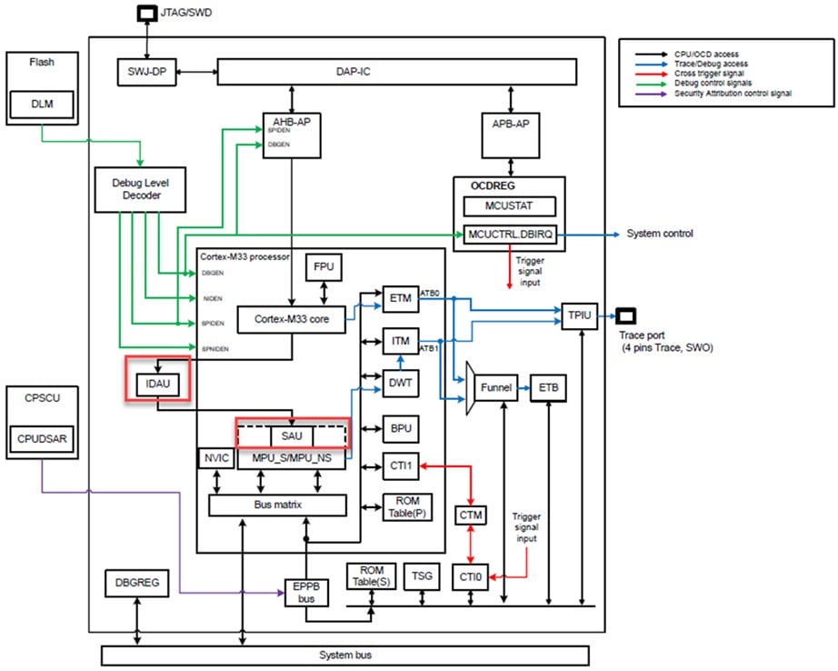
The TrustZone policy enforcement is responsibility of two dedicated responder units that get queried in parallel: the SAU (security attribution unit) and the IDAU (implementation-defined attribution unit). Both are highlighted in Figure 1 below.

Figure 1. Security attribution units (SAU, IDAU)
The SAU is software configurable and physically located within the CPU core; its implementation is defined by ARM. The IDAU is defined by a functional interface, the implementation being up to the silicon manufacturer. On each CPU memory transaction, both the SAU and IDAU perform an address lookup, and respond with the security attribute associated with the memory address. If an address maps to regions defined by both, their combined response will select the highest security level defined, as in Table 2.
Table 2. Highest security policy
| IDAU | SAU Region | Final Security Setting |
|---|---|---|
| S | X | S |
| X | S | S |
| NS | S-NSC | S-NSC |
| NS | NS | NS |
| S-NSC | NS | S-NSC |
Consequently, it is not possible to downgrade a “secure” or “secure non-secure callable” region to non-secure once an attribution unit has defined it as secure. This avoids a non-secure program getting access to a secure region by simply re-programming an SAU region (for example).
The CM33 secure extension additionally defines further aspects for each domain:
- separate interrupt vector tables
- separate stack pointers
- a dedicated “system tick” timer
- a dedicated MPU
Finally, there is a mechanism for controlled inter-domain communication.
A switch from a non-secure state to secure could happen once a secure interrupt occurs while the CPU is executing non-secure code. In such cases, the current CPU registers are pushed to the non-secure state, the CPU state is switched to secure, the secure stack pointer is used (all handled in hardware, automatically). Conversely, a switch from secure to non-secure could happen once a non-secure interrupt occurs when the CPU is executing secure code. In such scenario, the CPU register contents are first pushed on the secure stack, then cleared to zero by the hardware before the switch to the non-secure environment.
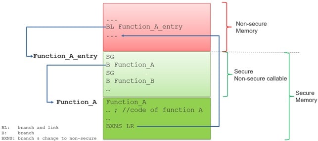
The isolated environment can be designed to provide ‘services’ to the non-secure application, allowing function calls from the non-secure environment, but the CPU needs to switch to secure mode first. This is done in a controlled way, via a special instruction called ‘secure gateway (SG)’. An SG instruction is paired with an immediately following branch instruction to the desired secure function address; this defines a “trampoline” for the non-secure application to first switch its state to secure (executing the SG first) and then jump to the desired secure function.
All pairs of ‘SG + Branch address’ instructions get allocated into a secure area which has the additional special attribute of being “non-secure callable”. Non-secure programs can only access the non-secure callable section within a secure memory area, and any direct branch into the non-secure callable area must target an SG instruction address; otherwise, a security exception gets generated.
When the secure function returns, the processor state is switched back to the non-secure mode by executing a special ‘branch return’ instruction. An example of application flow using the secure gateway instruction to call a secure API and return is shown in Figure 2.

Figure 2. Secure gateway program flow
It shall be noted that any function parameters (like memory buffer pointers) passed to a non-secure callable function shall be tested for their security attribute before usage, to ensure the caller has the proper access permissions over that memory area. For example, the secure function must check that the memory buffer pointer passed by the caller is in a non-secure memory area, and the buffer boundaries do not overlap a secure memory section. This can be done via a specialized instruction called ‘test target’. Proper usage of the test target instruction is the responsibility of the secure function, as appropriate. The Renesas tools available to configure a TZ project will generate appropriate ‘guard functions’ which can be used to implement such content checks in the code.
The last missing combination is for a change from secure to non-secure state, from secure code. The CPU, while in a secure state, can execute a branch (jump) instruction to a non-secure memory area, either directly, or to finalize the return flow from a previously called NSC function. The branch instruction switches the CPU state to NS, any return address is pushed to the secure stack. In such cases, the secure function is responsible for clearing the CPU registers as appropriate before executing the branch instruction.
The number of regions defined in the SAU is configurable in the Cortex‑M33 implementation to be either 0, 4, or 8. In the case of the RA6 and RA4 MCU family, the SAU is defined with 0 regions, therefore, not implemented. Some of the SAU control registers must always be implemented, and the RA MCU hardware user manual instructs to set the SAU_CTRL.ALLNS = 1b, changing the SAU default (background) response to non-secure. Consequently, the final security setting is determined by the IDAU solely. This configuration is applied by secure software during the initialization phase.
To configure the secure and non-secure memory boundaries (for flash, ram memory, and data flash), the RA series features a programmable IDAU. With such a design, partitioning the system boundaries is very easy and simple.
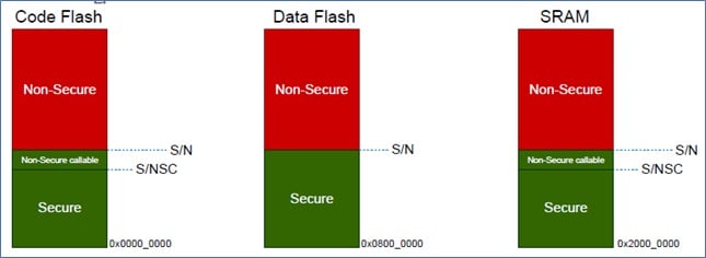
The default attribute for an undefined area by the IDAU is secure; otherwise, the security attribute corresponding to the IDAU setting is used. Depending on the memory type, a different type of granularity is allowed for the boundaries, as shown in Table 3.

Figure 3. Memory boundaries
Table 3. IDAU boundaries
| Boundary | Code Flash | Data Flash | SRAM |
|---|---|---|---|
| S/NS | 32 KB | 1 KB | 8 KB |
| S/NSC | 1 KB | - | 1 KB |
This ensures the amount of memory dedicated to the secure area and the non-secure callable area is optimized for efficiency. In most practical cases, the functionality provided in the secure environment is the minimal possible, reducing the scope of potential issues and erratic behavior, and making verification easier. A typical example of using the secure area in IoT devices is to implement isolated cryptographic services (key management, encryption/decryption and so on). In such cases, the goal is to reduce the ‘attack surface’ as much as possible and therefore, the non-secure callable area would typically be of the smallest size (the least number of APIs implemented). A 1 KB boundary shall be more than sufficient in most practical cases.
The user can define the memory boundaries by programming dedicated registers, located in an isolated, non-volatile flash memory area, memory mapped as read-only (to prevent application tampering). Programming of the IDAU register values is done using the MCU production programming interface (serial line, USB I/F, or other physical interfaces supported by the device) while programming the firmware application image in production. To activate the programming interface, the microcontroller must enter the “boot mode” of operation; this is selected by a low voltage level of MD pin at reset (the application software is always executed while in “single chip” mode).
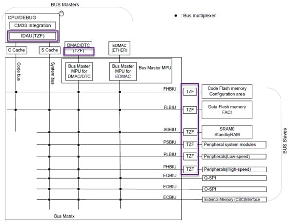
In addition to the CPU, the MCU must consider all other agents which can issue bus transactions (to/from memory, to/from memory-mapped peripherals), like Direct Memory Access (DMA) controllers, graphic engines, USB controllers, ethernet controllers, and so on. For this purpose, TrustZone ‘filters’ (see Figure 4) are implemented to monitor the bus transactions, allow the legitimate to proceed, and block the non-allowed ones.

Figure 4. TrustZone related filters
Each bus master has specific security attributes implemented to tag its generated transactions as secure or non-secure. An illegal transaction will generate a non-maskable interrupt (NMI) or a reset, depending on the user-defined configuration. Unauthorized write accesses are ignored (not performed), while reads always return zero. Illegal DMA transfers are either not started at all or stopped as soon as a violation is detected (like a buffer overflow).
On the endpoint side, each peripheral IP on the chip has a specific security attribute defining the access policy to its functional interface, implemented as memory-mapped system function registers (SFRs). There are different types of peripherals defined:
- Type-1 peripherals can be configured as secure or non-secure for all SFRs related to each channel or module.
- Type-2 peripherals have individual registers and/or bitfields configurable as secure, if, for example, system-level modules or I/F status registers need to be shared between both environments. The secure configured bitfields are protected from non-secure modifications.
For example, the RTC (real-time clock) is a type-1 peripheral since it is a single instance. The CAN controller interface is implemented as two-channel instances (CAN0 and CAN1), and each instance is treated as a type-1 peripheral. Other type-1 peripherals are multichannel, like GPTs (general purpose timers), and serial lines, like SCI (serial channel interface). Those do share few SFRs, but have a dedicated security attribute per each channel so that the application developer can choose which specific channel shall be specified as secure.
Type-2 peripherals typically control system-level settings (clock configuration, low power modes, etc.) and its SFRs need both secure and non-secure access capabilities. In such IPs, the security attributes are configured per bit. The GPIO interface is a special case, since each GPIO port groups several bit settings, there is a security attribute defined per each pin.
The reset vector (interrupt vector table) of the CPU is fixed to address 0x0 in memory. The processor fetches the reset vector and stack pointer automatically from the interrupt vector table at hardware reset, therefore the CPU always starts executing from the lower portion of flash memory where the secure boundary start is located.
Looking closer at Figure 4, one might notice that a few items do not have a TZ filter, for example, the external memory interfaces. In fact, external memory is classified as ‘non-secure’ from the programmer’s view, with an ‘exempt’ security attribute. An exempt region is not subject to security checks, and the SAU/IDAU settings have, in practice, no effect. This, in turn, means, there is no change of security status needed on the core side, it will just fetch and eventually execute instructions from external memory keeping the same mode. Even an SG instruction, will be treated as NOP, with no effect.
In such a scenario, it is impossible to protect the contents of the external device from tampering. Therefore, it is advised not to allocate and/or execute any secure code from external memory areas, since it can be modified easily, or executed while in a non-secure state. As an additional countermeasure, the secure MPU could be set to mark that area as ‘XN’ (execute never) to prevent instruction execution by mistake. It is out of assumption for a user to allocate secure code and NSC code (including SG instructions) in OSPI (for example), but that memory can be easily used to expand application level non-secure code as needed, or store firmware update images, or application data (encrypted or not).
As for the configuration of the application and the drivers, Renesas has developed a clever and simple-to-use tool, integrated within the E2Studio development environment, to guide the configuration of a secure and non-secure project in a few easy steps. Under the hood, the tool - in accordance with the FSP software - takes care of generating all appropriate compiler primitives and macros necessary for the HAL drivers, to handle the configured NSC calls and state transitions. It also assists in allocating the memory layout automatically in a size-optimized way and generating the secure and non-secure sections for later seamless programming of the application image.
