Overview
Description
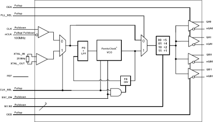
IDT's PLL-based clock generators offer sub-picosecond jitter, low-skew clock outputs, and edge rates that meet the ever-growing demands of today's networking solutions. The 871S1022 is a PLL-based clock generator specifically designed for PCI Express® Clock Generation applications. The device generates 100MHz, 125MHz, 250MHz or 500MHz from either a 25MHz fundamental mode crystal or a 100MHz recovered clock. The 871S1022 has two modes of operation: (1) high frequency jitter attenuator and (2) high performance clock synthesizer mode. When in jitter attenuator mode, the 871S1022 is able to both suppress high frequency noise components and function as a frequency translator. Designed to receive a jittery and noisy clock from an external source, the 871S1022 uses FemtoClock® technology to clean up the incoming clock and translate the frequency to one of the four common PCI Express® frequencies. When in synthesizer mode, the device is able to generate high performance SSC and non-SSC clocks from a low cost external, 25MHz, fundamental mode crystal. The 871S1022 uses FemtoClock® technology to generate low noise clock outputs capable of providing the seed frequencies for the common PCI Express® link rates.
Features
- Four 0.7V differential output pairs
- One differential clock input pair
- CLK, nCLK pair can accept the following differential input levels: LVPECL, LVDS, LVHSTL, HCSL
- Crystal oscillator interface designed for 25MHz, 18pF parallel resonant crystal
- RMS phase jitter @ 100MHz, using a 25MHz crystal (12kHz - 20MHz): 0.608ps (typical)
- High frequency jitter attenuator mode has high PLL bandwidth which allows for better input tracking
- Supports PCI Express® Spread-Spectrum Clocking
- PCI Express® Gen 1, 2 and 3 jitter compliant
- 3.3V operating supply voltage
- 0°C to 70°C ambient operating temperature
- Available in lead-free (RoHS 6) package
Comparison
Applications
Documentation
|
|
|
|
|---|---|---|
| Type | Title | Date |
| Datasheet | PDF 862 KB | |
| End Of Life Notice | PDF 938 KB | |
| End Of Life Notice | PDF 909 KB | |
| Product Change Notice | PDF 983 KB | |
| Product Change Notice | PDF 583 KB | |
| Product Change Notice | PDF 596 KB | |
| Product Change Notice | PDF 544 KB | |
7 items
|
||
Design & Development
Models
ECAD Models
Schematic symbols, PCB footprints, and 3D CAD models from SamacSys can be found by clicking on products in the Product Options table. If a symbol or model isn't available, it can be requested directly from the website.

Videos & Training
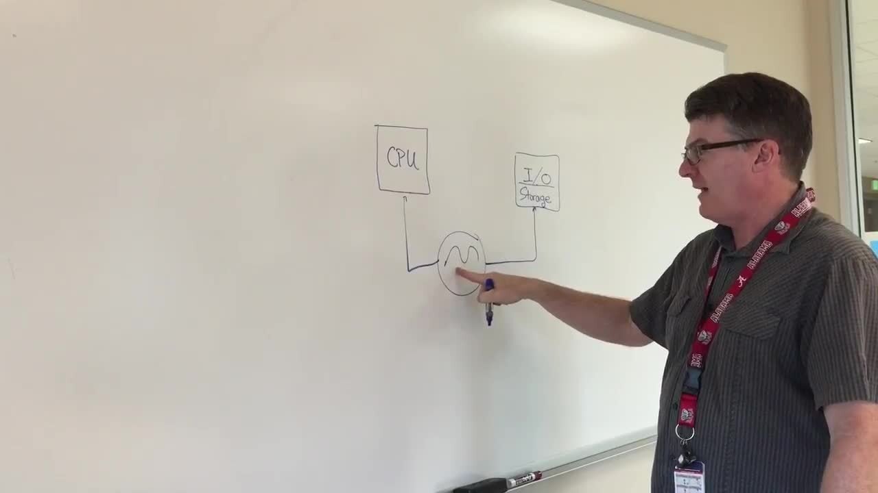
This is the first video in our PCIe series. In this video, we define PCIe architectures, focusing on common and separate clock architectures. Watch the rest of the video series below where Ron will cover the impact of different timing architectures.
Watch the Video Series Below


