Overview
Description
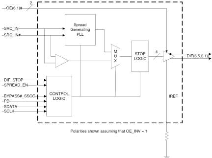
The 9DS400 is a 4-output PCIe PLL with the ability to inject spread spectrum onto the incoming differential clock, while maintaining good phase noise.
Features
- 4- 0.7V current-mode differential output pairs
- Supports Spread Injection mode and fanout mode
- Two pin selectable down spread amounts: 0.5% and 0.25%
- 50-110 MHz operation in PLL mode
- 50-400 MHz operation in Bypass mode
- Bypass mode
- Supports undriven differential outputs in PD# and SRC_STOP# modes for power management
- Output cycle-cycle jitter < 50ps
- Output to Output skew <50ps
- Phase jitter: PCIe Gen1 < 86ps peak to peak
- Phase jitter: PCIe Gen2 < 3.0/3.1ps rms
Comparison
Applications
Design & Development
Models
ECAD Models
Schematic symbols, PCB footprints, and 3D CAD models from SamacSys can be found by clicking on products in the Product Options table. If a symbol or model isn't available, it can be requested directly from the website.

Videos & Training
PCIe Clocking Architectures (Common and Separate)
This is the first video in our PCIe series. In this video, we define PCIe architectures, focusing on common and separate clock architectures. Watch the rest of the video series below where Ron will cover the impact of different timing architectures.
Watch the Video Series Below
Video List


