Overview
Description
Support is limited to customers who have already adopted these products.
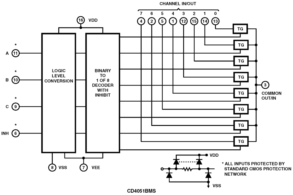
CD4051BMS, CD4052BMS and CD4053BMS analog multiplexers/ demultiplexers are digitally controlled analog switches having low ON impedance and very low OFF leakage current. Control of analog signals up to 20V peak-to-peak can be achieved by digital signal amplitudes of 4. 5V to 20V (if VDD-VSS = 3V, a VDD-VEE of up to 13V can be controlled; for VDD-VEE level differences above 13V, a VDDVSS of at least 4. 5V is required). For example, if VDD = +4. 5V, VSS = 0, and VEE = -13. 5V, analog signals from - 13. 5V to +4. 5V can be controlled by digital inputs of 0 to 5V. These multiplexer circuits dissipate extremely low quiescent power over the full VDD-VSS and VDD-VEE supply voltage ranges, independent of the logic state of the control signals. When a logic 1 is present at the inhibit input terminal all channels are off. The CD4051BMS is a single 8 channel multiplexer having three binary control inputs, A, B, and C, and an inhibit input. The three binary signals select 1 of 8 channels to be turned on, and connect one of the 8 inputs to the output. The CD4052BMS is a differential 4 channel multiplexer having two binary control inputs, A and B, and an inhibit input. The two binary input signals select 1 of 4 pairs of channels to be turned on and connect the analog inputs to the outputs. The CD4053BMS is a triple 2 channel multiplexer having three separate digital control inputs, A, B, and C, and an inhibit input. Each control input selects one of a pair of channels which are connected in a single pole double-throw configuration. The CD4051BMS, CD4052BMS and CD4053BMS are supplied in these 16 lead outline packages: Braze Seal DIP *H4X †H4T Frit Seal DIP H1E Ceramic Flatpack H6W *CD4051B Only †CD4052B, CD4053 Only
Features
- Logic Level Conversion
- High-Voltage Types (20V Rating)
- CD4051BMS Signal 8-Channel
- CD4052BMS Differential 4-Channel
- CD4053BMS Triple 2-Channel
- Wide Range of Digital and Analog Signal Levels:
- Digital 3V to 20V
- Analog to 20Vp-p
- Low ON Resistance: 125Ω (typ) Over 15Vp-p Signal Input Range for VDD - VEE = 15V
- High OFF Resistance: Channel Leakage of ±100pA (typ) at VDD - VEE = 18V
- Logic Level Conversion:
- Digital Addressing Signals of 3V to 20V (VDD - VSS = 3V to 20V)
- Switch Analog Signals to 20Vp-p (VDD - VEE = 20V); See Introductory Text
- Matched Switch Characteristics: RON = 5Ω (typ) for VDD - VEE = 15V
- Very Low Quiescent Power Dissipation Under All Digital Control Input and Supply Conditions: 0.2µW (typ) at VDD - VSS = VDD - VEE = 10V
- Binary Address Decoding on Chip
- 5V, 10V and 15V Parametric Ratings
- 100% Tested for Quiescent Current at 20V
- Maximum Input Current of 1µA at 18V Over Full Package Temperature Range; 100nA at 18V and +25°C
- Break-Before-Making Switching Eliminates Channel Overlap
Comparison
Applications
- Analog and Digital Multiplexing and Demultiplexing
- A/D and D/A Conversion
- Signal Gating
* When these devices are used as demultiplexers the "CHANNEL IN/OUT" terminals are the outputs and the "COMMON OUT/IN" terminals are the inputs
Documentation
Featured Documentation
Log in required to subscribe
|
|
|
|
|---|---|---|
| Type | Title | Date |
| Datasheet | PDF 447 KB | |
| Brochure | PDF 467 KB | |
| End Of Life Notice | PDF 93 KB | |
| Product Advisory | PDF 499 KB | |
| Product Change Notice | PDF 230 KB | |
5 items
|
||
Design & Development
Models
ECAD Models
Schematic symbols, PCB footprints, and 3D CAD models from SamacSys can be found by clicking on products in the Product Options table. If a symbol or model isn't available, it can be requested directly from the website.

Product Options
Applied Filters: