Overview
Description
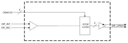
The IDT6V31021 is a 4-output low- power differential buffer. Each output has its own OE# pin. It has a maximum operating frequency of 167 MHz and supports all SERDES clock frequencies for Freescale QorIQ CPUs.
Features
- 4 - low power differential output pairs
- Individual OE# control of each output pair
- Low power differential outputs
- Power down mode when all OE# are high
- Industrial temperature range
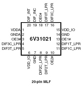
- 20-pin MLF
- Output cycle-cycle jitter <15 ps additive
- Output to Output skew: <50 ps
- PCIe Gen3 additive phase jitter <0.3 ps rms
- 10.3125G / 64 additive phase jitter <100 fs rms
Comparison
Applications
Design & Development
Models
ECAD Models
Schematic symbols, PCB footprints, and 3D CAD models from SamacSys can be found by clicking on products in the Product Options table. If a symbol or model isn't available, it can be requested directly from the website.

Videos & Training
PCIe Clocking Architectures (Common and Separate)
This is the first video in our PCIe series. In this video, we define PCIe architectures, focusing on common and separate clock architectures. Watch the rest of the video series below where Ron will cover the impact of different timing architectures.
Watch the Video Series Below
Video List


