Overview
Description
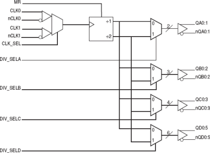
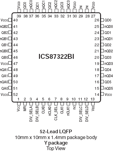
The 87322BI is a low skew, ÷1/÷2 3.3V LVPECL/ECL Clock Generator. Using multiplexed/redundant clock inputs the 87322BI is designed to translate most differential signal levels to LVPECL/ECL levels. The CLK_SEL input selects between CLK0, nCLK0 and CLK1, nCLK1 as the active input. The divide select inputs, DIV_SELA, DIV_SELB, DIV_SELC, DIV_SELD, control the output frequency of each bank. The outputs can be utilized in the ÷1, ÷2 or a combination of ÷1 and ÷2 modes. The master reset input can be used to reset the internal dividers and disable the clock outputs. Disabled outputs QAx, QBx, QCx and QDx will be forced low. Disabled outputs nQAx, nQBx, nQCx and nQDx will be forced high. The 87322BI is characterized across the industrial temperature range and over the supply voltage range of 3V to 3.8V for LVPECL and -3.8V to -3V for LVECL/ECL. Guaranteed output and part to part skew characteristics make the 87322BI an excellent choice for clock generator and clock distribution applications demanding well defined performance and repeatability.
Features
- Fifteen differential LVPECL outputs
- Selectable LVPECL differential clock inputs
- CLK0, nCLK0 and CLK1, nCLK1 can accept the following differential input levels: LVPECL, LVDS, CML, SSTL
- Output frequency: 750MHz (maximum)
- Output skew: 180ps (maximum)
- Bank skew: 65ps (maximum)
- Part-to-part skew: 500ps (maximum)
- LVPECL mode operating voltage supply range: VCC = 3V to 3.8V, VEE = 0V
- ECL mode operating voltage supply range: VCC = 0V, VEE = -3.8V to -3V
- -40°C to 85°C ambient operating temperature
- Lead-Free package fully RoHS compliant
Comparison
Applications
Design & Development
Models
ECAD Models
Schematic symbols, PCB footprints, and 3D CAD models from SamacSys can be found by clicking on products in the Product Options table. If a symbol or model isn't available, it can be requested directly from the website.


