Overview
Description
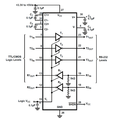
The ISL4260E contains 3. 0V to 5. 5V powered RS‑232 transmitters/receivers that meet ElA/TIA-232 and V. 28/V. 24 specifications, even at VCC = 3. 0V. Targeted applications are PDAs, Palmtops, and cell phones where the low operational power consumption and even lower standby power consumption is critical. Efficient on-chip charge pumps coupled with a manual powerdown function reduces the standby supply current to a 150nA trickle. The 5mm x 5mm Quad Flat No-Lead (QFN) packaging and the use of small, low value capacitors ensure board space savings. Data rates greater than 250kbps are ensured at worst case load conditions. The ISL4260E features a VL pin that adjusts the logic pin output levels (see Pin Descriptions) and input thresholds to values compatible with the VCC powering the external logic (for example, a UART). The single pin powerdown function (SHDN = 0) disables all the receiver and transmitter outputs while shutting down the charge pump to minimize supply current drain. Application Note AN9863 summarizes the features of each device comprising the 3V RS-232 family.
Features
- Available in near chip scale QFN (5mmx5mm) package
- VL pin for compatibility with mixed voltage systems
- ESD protection for RS-232 I/O pins to ±15kV (IEC61000)
- Single SHDN pin disables transmitters and receivers
- Meets EIA/TIA-232 and V.28/V.24 specifications at 3V
- On-chip charge pumps require only four external 0.1µF capacitors
- Receiver hysteresis for improved noise immunity
- Very low supply current: 300µA
- Guaranteed minimum data rate: 250kbps
- Wide power supply range: Single +3V to +5.5V
- Low supply current in powerdown state: 150nA
- Pb-free (RoHS compliant)
Comparison
Applications
- Any System Requiring RS-232 Communication Ports Battery Powered, Hand-Held, and Portable Equipment Laptop Computers, Notebooks, Palmtops Digital Cameras PDAs and PDA Cradles Cellular/Mobile Phones
Design & Development
Models
ECAD Models
Schematic symbols, PCB footprints, and 3D CAD models from SamacSys can be found by clicking on products in the Product Options table. If a symbol or model isn't available, it can be requested directly from the website.


