Overview
Description
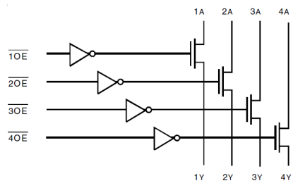
The QS3VH125 is a high-bandwidth, quad bus switch. The QS3VH125 has very low ON-resistance, resulting in under 250ps propagation delay through the switch. The switches can be turned ON under the control of individual LVTTL-compatible active low Output Enable signals for bidirectional data flow with no added delay or ground bounce. The combination of near-zero propagation delay, high OFF impedance, and overvoltage tolerance makes the QS3VH125 ideal for high-performance communications applications. The QS3VH125 operates from -40 °C to +85 °C.
Features
- N-channel FET switches with no parasitic diode to VCC
- Isolation under power-off conditions
- No DC path to VCC or GND
- 5V tolerant in OFF and ON state
- 5V tolerant I/Os
- Low RON - 4Ω typical
- Flat RON characteristics over operating range
- Rail-to-rail switching 0V to 5V
- Bidirectional dataflow with near-zero delay: No added ground bounce
- Excellent RON matching between channels
- VCC operation: 2.3V to 3.6V
- High bandwidth - Up to 500MHz
- LVTTL-compatible control inputs
- Undershoot clamp diodes on all switch and control inputs
- Low I/O capacitance, 4pF typical
- Available in 16-pin QSOP and 14-pin SOIC packages
Comparison
Applications
- Hot-swapping
- 10/100 Base-T, Ethernet LAN switch
- Low distortion analog switch
- Replaces mechanical relay
- ATM 25/155 switching
Design & Development
Models
ECAD Models
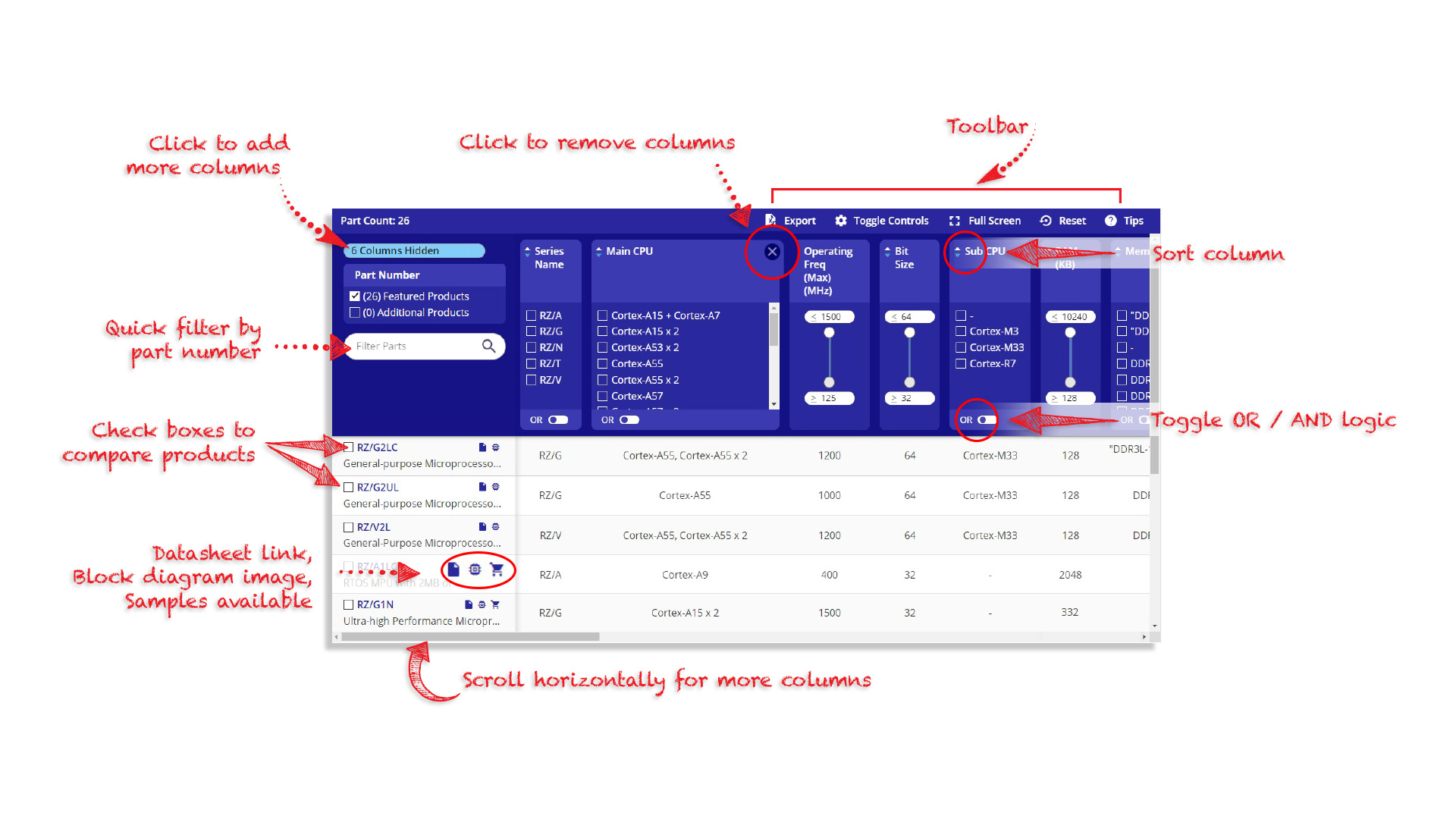
Schematic symbols, PCB footprints, and 3D CAD models from SamacSys can be found by clicking on products in the Product Options table. If a symbol or model isn't available, it can be requested directly from the website.


