Overview
Description
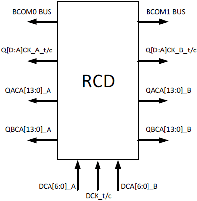
The RG5R256 (Gen 2 RCD) is a registering clock driver used on DDR5 RDIMMs, LRDIMMs and NVDIMMs. It supports DDR5 server speeds up to 5600 MT/s. Its primary function is to buffer the Command Address (CA) bus, chip selects, and clock between the host controller and the DRAMs. It also creates a BCOM bus to control the data buffers for LRDIMMs.
The RG5R256 contains two separate channels with some common logic such as clocking, but otherwise operate independently of each other. Each channel has a 7-bit double data rate CA bus input, a single parity input, two chip-select inputs, produces two copies of 14-bit single data rate CA bus outputs and two copies of the chip-select outputs. The RCD has a common clock input and PLL, but produces separate clock outputs to the DRAM channels.
Features
- Pinout optimized DDR5 RDIMM and LRDIMM PCB layout
- DDR5 server speeds up to 5600MT/s
- Supports power-down modes to conserve server power
- Supports 1-rank/2-rank DIMM configurations
- Supports SDP, DDP, 3DS DRAM types
- Supports up to 16Gb DRAM die
- Provides access to internal control words for configuring device features and adapting to different RDIMM and LRDIMM system applications
- I2C and I3C sideband access for register access control
- BCOM for LRDIMM data buffer control
- Loopback and pass-through modes
- Package: 8.7 × 13.5 mm, 240-FCBGA
Comparison
Applications
- RDIMM, LRDIMM and NVDIMM modules for Enterprise Servers
- Memory down server motherboards
Documentation
|
|
|
|
|---|---|---|
| Type | Title | Date |
| Datasheet - Short-Form | PDF 159 KB | |
| Product Change Notice | PDF 925 KB | |
| Product Change Notice | PDF 924 KB | |
| Product Change Notice | PDF 291 KB | |
4 items
|
||
Design & Development
Models
ECAD Models
Schematic symbols, PCB footprints, and 3D CAD models from SamacSys can be found by clicking on products in the Product Options table. If a symbol or model isn't available, it can be requested directly from the website.

Product Options
Applied Filters:
