Overview
Description
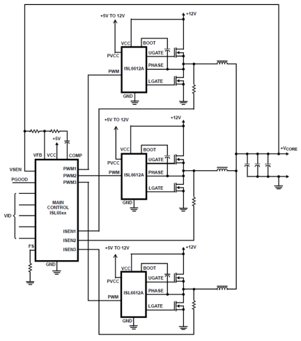
The ISL6612A and ISL6613A are high frequency MOSFET drivers specifically designed to drive upper and lower power N-Channel MOSFETs in a synchronous rectified buck converter topology. These drivers combined with HIP63xx or ISL65xx Multi-Phase Buck PWM controllers and N-Channel MOSFETs form complete core-voltage regulator solutions for advanced microprocessors. The ISL6612A drives the upper gate to 12V, while the lower gate can be independently driven over a range from 5V to 12V. The ISL6613A drives both upper and lower gates over a range of 5V to 12V. This drive-voltage provides the flexibility necessary to optimize applications involving trade-offs between gate charge and conduction losses. An advanced adaptive zero shoot-through protection is integrated to prevent both the upper and lower MOSFETs from conducting simultaneously and to minimize the dead time. These products add an overvoltage protection feature operational before VCC exceeds its turn-on threshold, at which the PHASE node is connected to the gate of the low side MOSFET (LGATE). The output voltage of the converter is then limited by the threshold of the low side MOSFET, which provides some protection to the microprocessor if the upper MOSFET(s) is shorted during initial startup. These drivers also feature a three-state PWM input which, working together with multi-phase PWM controllers, prevents a negative transient on the output voltage when the output is shut down. This feature eliminates the Schottky diode that is used in some systems for protecting the load from reversed output voltage events.
Features
- Pin-to-pin Compatible with HIP6601 SOIC family
- Dual MOSFET Drives for Synchronous Rectified Bridge
- Advanced Adaptive Zero Shoot-Through Protection
- Body Diode Detection
- Auto-zero of rDS(ON) Conduction Offset Effect
- Adjustable Gate Voltage (5V to 12V) for Optimal Efficiency
- 36V Internal Bootstrap Schottky Diode
- Bootstrap Capacitor Overcharging Prevention
- Supports High Switching Frequency (up to 2MHz)
- 3A Sinking Current Capability
- Fast Rise/Fall Times and Low Propagation Delays
- Three-State PWM Input for Output Stage Shutdown
- Three-State PWM Input Hysteresis for Applications with Power Sequencing Requirement
- Pre-POR Overvoltage Protection
- VCC Undervoltage Protection
- Expandable Bottom Copper Pad for Enhanced Heat Sinking
- Dual Flat No-Lead (DFN) Package
- Near Chip-Scale Package Footprint; Improves PCB Efficiency and Thinner in Profile
- Pb-Free (RoHS Compliant)
Comparison
Applications
- Core Regulators for Intel® and AMD® Microprocessors
- High Current DC/DC Converters
- High Frequency and High Efficiency VRM and VRD
Design & Development
Models
ECAD Models
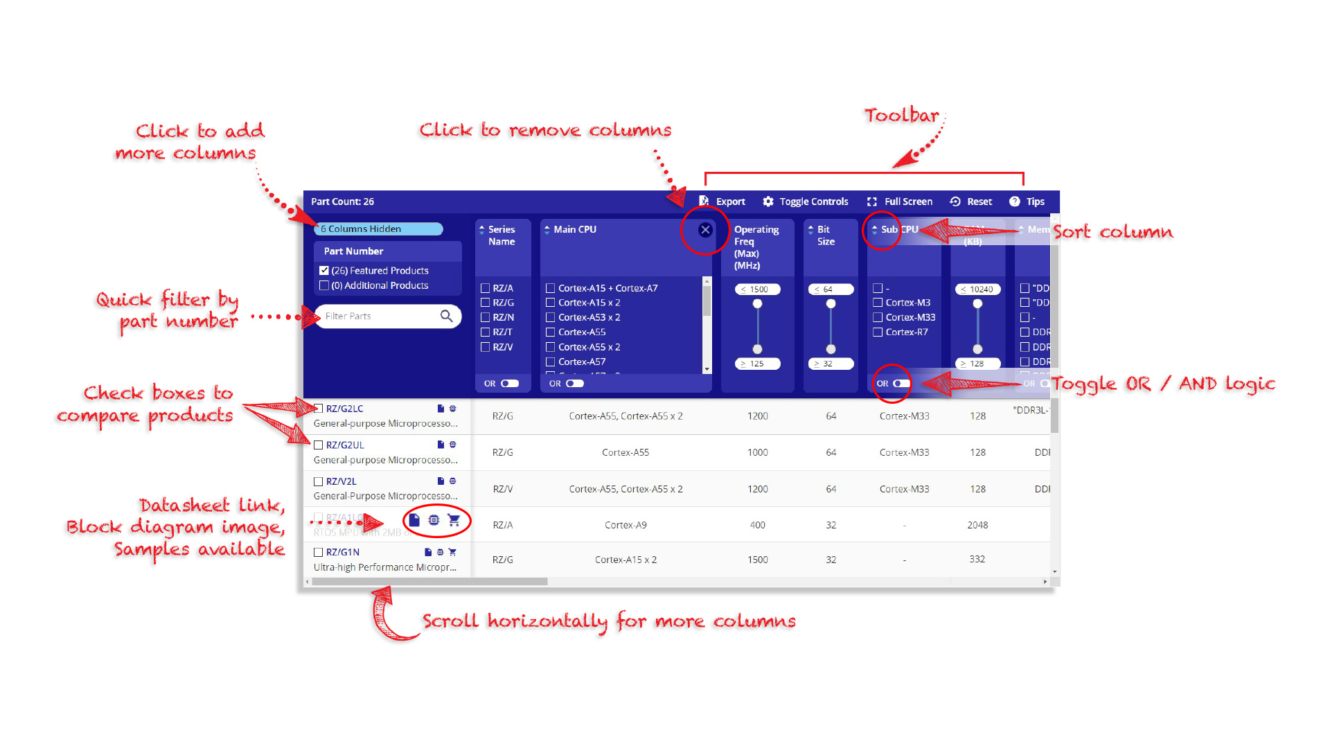
Schematic symbols, PCB footprints, and 3D CAD models from SamacSys can be found by clicking on products in the Product Options table. If a symbol or model isn't available, it can be requested directly from the website.


