Overview
Description
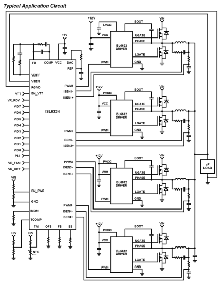
The ISL6622 is a high frequency MOSFET driver designed to drive upper and lower power N-Channel MOSFETs in a synchronous rectified buck converter topology. The advanced PWM protocol of ISL6622 is specifically designed to work with Intersil VR11. 1 controllers and combined with N-Channel MOSFETs, form a complete core-voltage regulator solution for advanced microprocessors. When ISL6622 detects a PSI protocol sent by an Intersil VR11. 1 controller, it activates Diode Emulation (DE) and Gate Voltage Optimization Technology (GVOT) operation; otherwise, it operates in normal Continuous Conduction Mode (CCM) PWM mode. In the 8 Ld SOIC package, the ISL6622 drives the upper and lower gates to VCC during normal PWM mode, while the lower gate drops down to a fixed 5. 75V (typically) during PSI mode. The 10 Ld DFN part offers more flexibility: the upper gate can be driven from 5V to 12V via the UVCC pin, while the lower gate has a resistor-selectable drive voltage of 5. 75V, 6. 75V, and 7. 75V (typically) during PSI mode. This provides the flexibility necessary to optimize applications involving trade-offs between gate charge and conduction losses. To further enhance light load efficiency, the ISL6622 enables diode emulation operation during PSI mode. This allows Discontinuous Conduction Mode (DCM) by detecting when the inductor current reaches zero and subsequently turning off the low side MOSFET to prevent it from sinking current. An advanced adaptive shoot-through protection is integrated to prevent both the upper and lower MOSFETs from conducting simultaneously and to minimize dead time. The ISL6622 has a 20kΩ integrated high-side gate-to-source resistor to prevent self turn-on due to high input bus dV/dt. This driver also has an overvoltage protection feature operational while VCC is below the POR threshold: the PHASE node is connected to the gate of the low side MOSFET (LGATE) via a 10kΩ resistor, limiting the output voltage of the converter close to the gate threshold of the low side MOSFET, dependent on the current being shunted, which provides some protection to the load should the upper MOSFET(s) become shorted.
Features
- Dual MOSFET Drives for Synchronous Rectified Bridge
- Advanced Adaptive Zero Shoot-through Protection
- Integrated LDO for Selectable Lower Gate Drive Voltage (5.75V, 6.75V, 7.75V) to Optimize Light Load Efficiency
- 36V Internal Bootstrap Diode
- Advanced PWM Protocol (Patent Pending) to Support PSI Mode, Diode Emulation, Three-State Operation
- Diode Emulation for Enhanced Light Load Efficiency
- Bootstrap Capacitor Overcharging Prevention
- Supports High Switching Frequency
- 3A Sinking Current Capability
- Fast Rise/Fall Times and Low Propagation Delays
- Integrated High-Side Gate-to-Source Resistor to Prevent from Self Turn-On due to High Input Bus dV/dt
- Pre-POR Overvoltage Protection for Start-up and Shutdown
- Power Rails Undervoltage Protection
- Expandable Bottom Copper Pad for Enhanced Heat Sinking
- Dual Flat No-Lead (DFN) Package
- Near Chip-Scale Package Footprint; Improves PCB Efficiency and Thinner in Profile
- Pb-Free (RoHS Compliant)
Comparison
Applications
- High Light Load Efficiency Voltage Regulators
- Core Regulators for Advanced Microprocessors
- High Current DC/DC Converters
- High Frequency and High Efficiency VRM and VRD
Design & Development
Models
ECAD Models
Schematic symbols, PCB footprints, and 3D CAD models from SamacSys can be found by clicking on products in the Product Options table. If a symbol or model isn't available, it can be requested directly from the website.


