Is there anyone who has a problem with board design or noise countermeasure for products that use a MCU? As noise could cause a significant increase in cost and delay in product development, it is necessary to take sufficient measures in advance.
This time I have updated the "RX Family Hardware Design Guide" application note (R01AN1411).
In this Application Note, the connection between the MCU and main peripheral circuits such as the power supply circuit, clock circuit and reset circuit, and precaution notes when designing the board are explained in an easy to understand manner with the following layout examples.
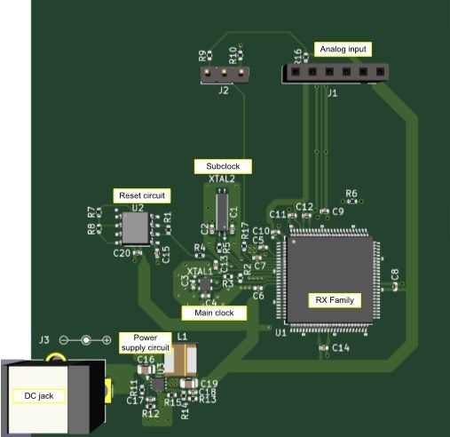
Component Layout (Front Side)
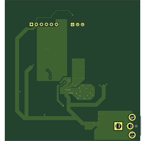
Component Layout (Back Side)
The followings are examples of wiring patterns for two-layer and four-layer boards. By using the wiring pattern diagrams designed with CAD software, the Application Note makes it easier to understand and imagine the actual board design.
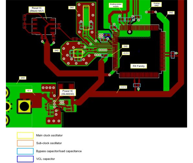
Example Wiring Pattern (Two-Layer Board)
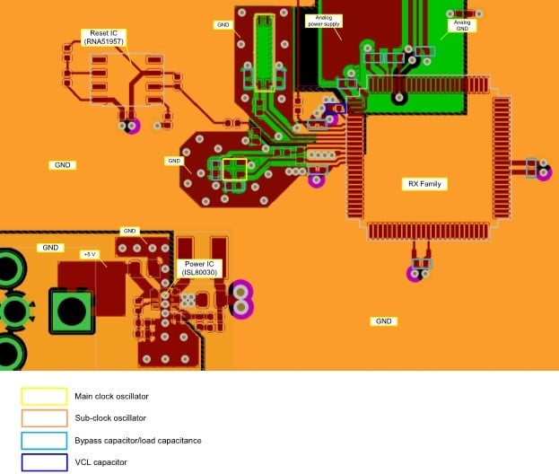
Example Wiring Pattern (Four-Layer Board)
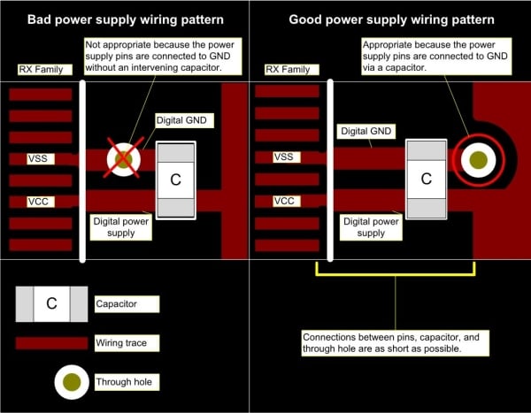
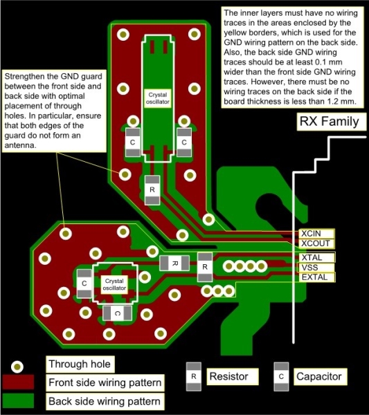
This Application Note picks up the particularly important peripheral such as power supply pins, reset pin, and clock I/O pins and, explain how to arrange wiring traces and through holes, and prenotes on board design for noise suppression.
Example Connections of Power Supply Pins
Example Clock I/O Pin Wiring Pattern
Please refer to this Application Note for your board design. Click here for the Application Note link.
