Overview
Description
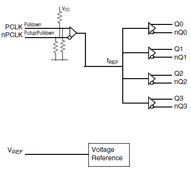
The 8SLVP1104I is a high-performance differential LVPECL fanout buffer designed for the fanout of high-frequency, very-low additive phase noise clock and data signals. The 8SLVP1104I is characterized for operation from a 3.3V or 2.5V power supply. Guaranteed output-to-output and part-to-part skew characteristics make the 8SLVP1104I ideal for clock distribution applications demanding well-defined performance and repeatability. Four low-skew outputs are available. The integrated bias voltage reference enables easy interfacing of single-ended signals to the device inputs. The device is optimized for low-power consumption and low-additive phase noise.

Features
- Four low-skew, low additive jitter LVPECL differential output pairs
- Differential LVPECL input pair can accept the following differential input levels: LVDS, LVPECL, CML
- Differential PCLKx pairs can also accept single-ended LVCMOS levels
- Maximum input clock frequency: 2GHz
- LVCMOS interface levels for the control input (input select)
- Output skew: 5ps (typical)
- Propagation delay: 320ps (maximum)
- Low additive phase jitter, RMS; fREF = 156.25MHz, VPP = 1V, 12kHz to 20MHz: 40fs (maximum)
- Maximum device current consumption (IEE): 60mA (maximum)
- Full 3.3V or 2.5V supply voltage
- Lead-free (RoHS 6) packaging
- -40 °C to 85 °C ambient operating temperature
Comparison
Applications
Design & Development
Software & Tools
Models
ECAD Models
Schematic symbols, PCB footprints, and 3D CAD models from SamacSys can be found by clicking on products in the Product Options table. If a symbol or model isn't available, it can be requested directly from the website.

Processing table
| VFQFPN | 16 | I | Yes | Tray | 3 | 3.984 | Get Samples, | |
| VFQFPN | 16 | I | Yes | Reel | 3 | 4.14 |
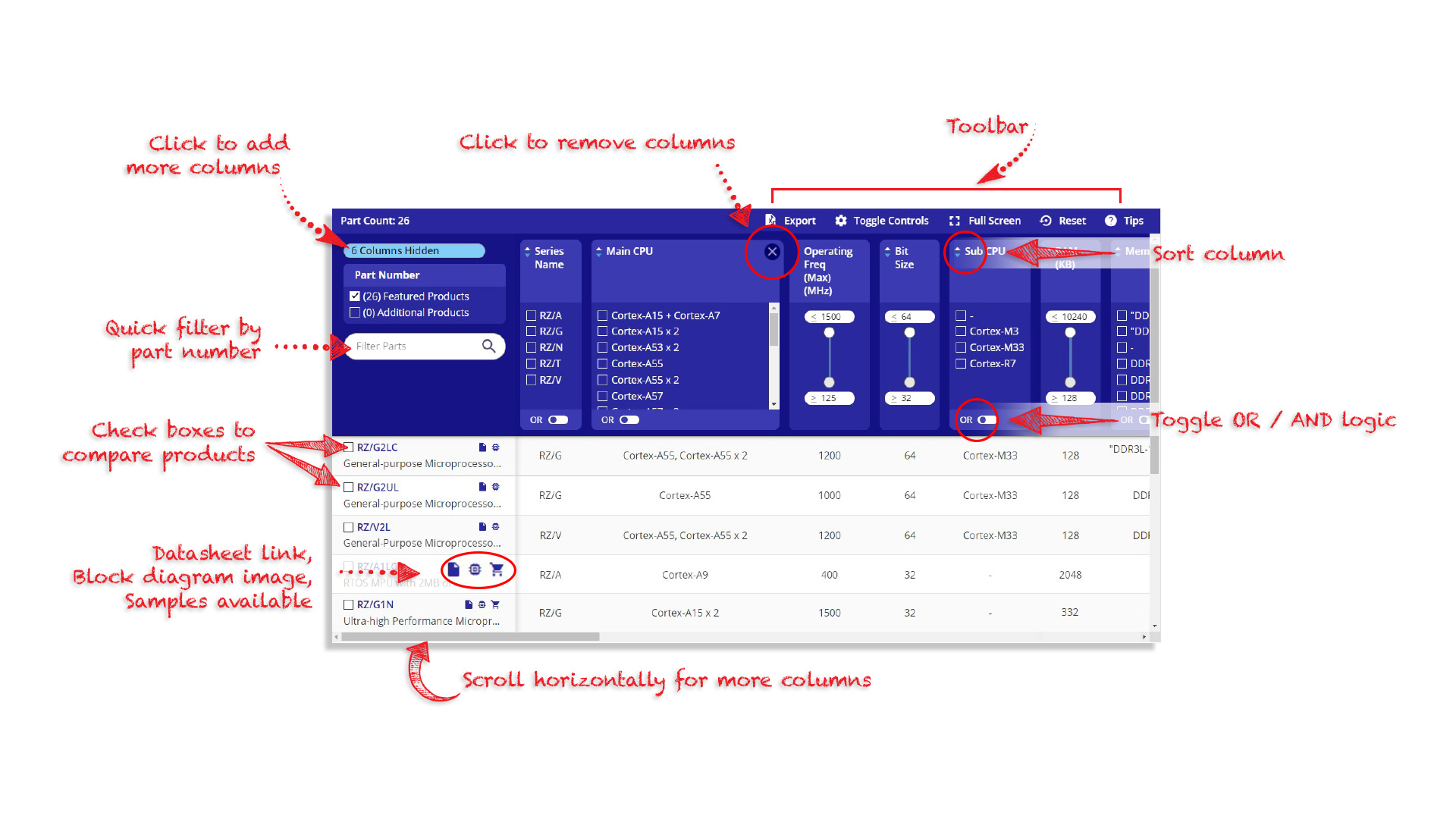
Tips for Using This Parametric Table:
- Hide Filters button in header: Collapse or expands filters
- Column sort buttons in header: Sort Column alphabetically / numerically descending or ascending
- Reset button in header: Reset all filters to the page default
- Full Screen button in header: Expand the table to full screen view (user must close out of full screen before they can interact with rest of page)
- Export button in header: Export the filtered results of the table to an Excel document
- Filter parts search bar in header: Type to filter table results by part number
- Hide column button in column headers: Select to hide columns in table
- AND / OR toggle switches in header: Toggles the logic of this particular filter to be “AND” or “OR” logic for filtering results
- Multiselect checkboxes at beginning of each row in table: Select these checkboxes to compare products against each other
- Document icon next to product name in row: View the featured document for this product
- Chip icon next to the right of the document icon in row: View the block diagram for this product
- Cart icon to the right of the chip icon: Indicates that samples are available for this product
Videos & Training
Low-jitter Differential Fanout Buffers - 8SLVP and 8SLVD Families from IDT
Description
Overview of IDT's 8LSVP (LVPECL) and 8SLVD (LVDS) families of low-jitter fanout buffers from IDT. Fanout buffers are a useful building block of many clock trees, providing signal buffering and multiple low-skew copies of the input signal. IDT's high-performance, low additive phase noise, differential clock fan-out buffers offer up to 2 GHz clock operation, low additive phase jitter (12kHz - 20MHz) of 50 to 100 femtoseconds RMS max, fast output rise & fall times (less than 150ps), and single and dual channel functions (dual: matched propagation delay). Presented by Baljit Chandhoke, Product Marketing Manager at Integrated Device Technology, Inc. To learn more about IDT's industry-leading portfolio of fanout buffers, visit Renesas's RF Buffer page.
Transcript
Hello. My name is Baljit Chandhoke and I'm the product marketing manager of clocking products at IDT. Today, I'll be giving you a brief overview of high performance differential clock fanout buffer family IDT 8SLVP family of LVPECL Buffers and IDT 8SLVD family of LVDS Buffers.
Clocks are the basic building blocks for all electronics today. Clock buffers are useful building block of clock trees because they're used to create multiple copies of the input clocks. Since clocks are used to drive processors and to synchronize the transfer of data between system components, the clock distribution system is an essential part of the system design. Hence, identifying the correct clock buffer for a system is extremely important. The key benefits of clock buffers are extreme low additive phase noise to drive jitter sensitive devices. Reduction in board space with reduced bill of material.
Key application of clock buffers: networking, computing, base stations, high end consumer, industrial communications, and instrumentation. Application issues solved by clock buffers: clock fanout to reduce bulk bill of material and board space. Fanout buffers enable frequency synchronized clock outputs to the same clock input reference. Fanout buffers enable low output to output skew between clock outputs. Low propagation delay between input and output clock. Low additive clock jitter at the output clock.
Now I'll talk about the 8SLVP family of LVPECL clock fanout buffers. These are high performance differential LVPECL clock fanout buffers with best in class extremely low additive phase-jitter. They are characterized to operate with a power supply of 3.3 volts and 2.5 volts. Guaranteed output-to-output and part-to-part skew characteristics make the 8SLVP family ideal for clock distribution applications demanding to modeling well-defined performance and repeatability.
The features of 8SLVP family of LVPECL fanout buffers are two selectable differential clock inputs which can accept LVPECL, LVDS or CML inputs. Output skew of 28ps. Propagation delay, 410ps. Low additive phase jitter with a RMS phase jitter of 54.1fs maximum. The device operates with a 3.3 volt and 2.5 volt power supply and operating temperature range of minus 40 degrees Celsius to 85 degrees Celsius.
IDT8SLVP family of LVPECL buffers is offered in different output configurations, with one to two fanouts to one to 12 fanouts. Dual channel options are available with dual one to four fanouts, dual one to eight fanouts. All these devices can operate with an input frequency up to 2 GHz with extremely low additive phase jitter of 50 to 100 fs RMS max. This device family has extremely fast output rise and fall time, with less than 150ps.
Now I'm going to talk about the 8SLVD family of LVDS fanout buffers. This family has optimized for low power consumption small output to output skew and propagation delay and best in class very low additive phase jitter. The key features of this family are two selectable clock inputs which can accept LVPECL or LVDS inputs. Maximum input clock frequency up to 2 GHz. Output skew 20ps max. Propagation delay 300ps. Low additive phase jitter, 95fs. This device family operates with a 2.5 volt supply voltage with some devices being offered with 3.3 volt power supply as well.
This slide shows you the family of devices. We offer LVDS fanout buffers with one to two fanout, dual channel one to two, one to four fanout. Dual channel one to four all the way up to one to 12 fanout buffers, with extremely low additive phase jitter, between 50 and 100fs.
In summary 8SLVP and 8SLVD family is a high performance differential LVPECL and LVDS fanout buffer family from IDT with best in class low additive clock jitter with 50 to 100fs RMS max. Low power consumption, small propagation delay, low output to output skew, fast rise time and fall time. IDT offers an extensive portfolio of single channel and dual channel LVPECL and LVDS fanout buffers from two outputs to 12 outputs.
We provide a complete product support with datasheets, timing solutions book, fanout buffer flyers on IDT website. In addition to the 8SLVP and 8SLVD family of fanout buffers we have the largest portfolio of fanout buffers with over 400 devices. IDT is committed to helping our customers with schematic reviews, IBIS or HSpice Models, well-established networks of FAEs in all geographies. Application notes on topics, layout guidelines, crystal selections, power supply filtering. For more information you can contact the link shown. Thank you for your time.
Video List