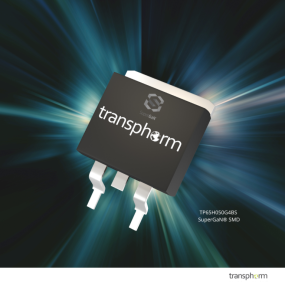
GOLETA, Calif. — Transphorm, Inc. (Nasdaq: TGAN)—a pioneer in and global supplier of high reliability, high performance gallium nitride (GaN) power conversion products—today announced the expansion of its surface mount package offerings with the addition of the TP65H050G4BS. The new higher-power surface mount device (SMD) is a 650V SuperGaN® FET in a TO-263 (D2PAK) offering a typical on-resistance of 50 milliohms. It marks Transphorm's seventh SMD, adding to a wide range of currently available PQFN devices for lower- to mid-power applications.
The JEDEC-qualified TP65H050G4BS offers several advantages to designers and manufacturers developing high power (single-to-multi-kilowatt) systems typically used in data center and broad industrial applications. It delivers Transphorm's best-in-class reliability, gate robustness (±20 Vmax), and silicon noise immunity threshold (4V) along with the ease of design and drivability synonymous with its GaN technology. Engineers use the larger D2PAK where both higher power and surface mount packaging is needed, enabling better thermal performance versus. PQFN type packages while increasing the efficiency of PCB assembly through the use of a single manufacturing flow.
Available as a discrete device, the D2PAK is also provided on a vertical daughter card to increase the power density of Transphorm's TDTTP2500B066B-KIT—a 2.5 kW AC-to-DC bridgeless totem pole power factor correction (PFC) evaluation board. It can also be swapped into the 1.2 kW synchronous half-bridge TDHBG1200DC100-KIT evaluation board to drive multi-kilowatt power.
"The D2PAK is an important addition to our portfolio. It expands the usability of our SMDs to high power applications, where before we supported these with through-hole devices," said Philip Zuk, SVP of Worldwide Marketing, Applications, and Business Development, Transphorm. "It's another step in helping customers leverage our GaN platform's advantages with familiar TO-XXX packages that eliminate design challenges, simplify system development, and quicken go-to-market ramps."
Transphorm is the only GaN supplier currently offering high voltage GaN devices in standard TO-XXX packages. Notably, these packages cannot be used with alternative e-mode GaN technology given its inherent gate sensitivity to damage.
Availability
The abovementioned device and evaluation boards are available from Digi-Key and Mouser via the links below:
- TP65H050G4BS FET: Digi-Key / Mouser
- 2.5 kW evaluation board: Digi-Key / Mouser
- 1.2 kW evaluation board: Digi-Key / Mouser
About Transphorm
Transphorm, Inc., a global leader in the GaN revolution, designs and manufactures high performance and high reliability GaN semiconductors for high voltage power conversion applications. Having one of the largest Power GaN IP portfolios of more than 1,000 owned or licensed patents, Transphorm produces the industry's first JEDEC and AEC-Q101 qualified high voltage GaN semiconductor devices. The Company's vertically integrated device business model allows for innovation at every development stage: design, fabrication, device, and application support. Transphorm's innovations are moving power electronics beyond the limitations of silicon to achieve over 99% efficiency, 40% more power density and 20% lower system cost. Transphorm is headquartered in Goleta, California and has manufacturing operations in Goleta and Aizu, Japan. For more information, please visit www.transphormusa.com. Follow us on Twitter @transphormusa and WeChat @ Transphorm_GaN.
The SuperGaN mark is a registered trademark of Transphorm, Inc. All other trademarks are the property of their respective owners.
The content in the press release, including, but not limited to, product prices and specifications, is based on the information as of the date indicated on the document, but may be subject to change without prior notice.
