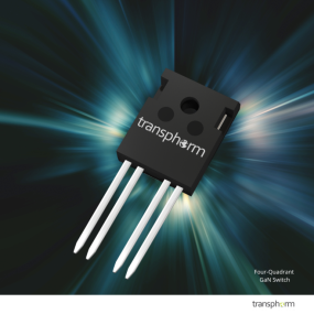
GOLETA, Calif. — Transphorm, Inc. (Nasdaq: TGAN)—a pioneer in and a global supplier of high reliability, high performance gallium nitride (GaN) power conversion products—announced today that it has been awarded a contract by the Advanced Research Projects Agency-Energy (ARPA-E). Part of the ARPA-E CIRCUITS program and through a sub-contract from Illinois Institute of Technology, the project covers the supply of GaN-based four-quadrant switches (FQSes) for use in various power conversion applications including novel ones like current source inverters, cyclo-converters for drives and microinverters, matrix switching, and solid-state circuit breakers. The initiative is the result of Transphorm's deep GaN engineering expertise (specifically its bidirectional GaN) along with industry and university interest in further exploring the possibilities of lateral GaN switches.
Transphorm will prototype the FQS platform using its 650 V GaN technology that continues to offer the industry's highest threshold voltage (4 V) in a 4-pin TO-247 package. The project is expected to be completed in less than a year.
The Importance of True Bidirectional GaN Switch Innovation
Transphorm's standard lateral GaN FETs inherently provide bidirectional current flow. However, certain applications such as current source inverters for motor drives, cyclo-converters and matrix converters also require bidirectional voltage control to effectively manage power flow. This capability is traditionally achieved by placing two FETs in series using the devices' body diode to steer and control current flow or via two IGBTs and two diodes, thus requiring four devices.
Also called a true bidirectional switch, the FQS replaces the two FET or the two IGBT+two diode approaches with a single device capable of realizing bidirectional voltage control and bidirectional current flow. The FQS uses two gates to block voltage of either polarity or pass current in either direction. And, as a single device, it reduces parts required to achieve the desired result thereby enabling higher power density, increased reliability, and overall system cost reduction.
"It is exciting to see the day approaching when GaN-based bidirectional switches will be ready for commercial production," says Emeritus Professor Tom Jahns, FIEEE, NAE, at the University of Wisconsin -Madison. "Power electronics engineers have been anxiously anticipating the day when MOS-gated bidirectional switches will become available because they are the key to implementing promising power converter topologies that offer exciting opportunities for improving efficiency, power density, and fault tolerance in many applications. They hold the potential to dramatically improve the commercial viability of new products including solid-state circuit breakers and integrated motor drives by making them significantly more compact and efficient than what is achievable using today's silicon-based switches."
"GaN adoption is at a point today when bringing an FQS bidirectional device to market makes sense," said Dr. Rakesh Lal, Technical Fellow at Transphorm. "Lateral GaN technology enables compact FQS dies to be fabricated because the voltage blocking region can be shared. This configuration cannot be realized with vertical power device technologies, such as with silicon or silicon carbide, which gives GaN FQSes a clear edge in performance and cost. With our FQS, one gets true bidirectionality in a fast low-loss switch, which we believe will inspire next generation power conversion products through the CIRCUITS program driven partnerships."
About Transphorm
Transphorm, Inc., a global leader in the GaN revolution, designs and manufactures high performance and high reliability GaN semiconductors for high voltage power conversion applications. Having one of the largest Power GaN IP portfolios of more than 1,000 owned or licensed patents, Transphorm produces the industry's first JEDEC and AEC-Q101 qualified high voltage GaN semiconductor devices. The Company's vertically integrated device business model allows for innovation at every development stage: design, fabrication, device, and application support. Transphorm's innovations are moving power electronics beyond the limitations of silicon to achieve over 99% efficiency, 40% more power density and 20% lower system cost. Transphorm is headquartered in Goleta, California and has manufacturing operations in Goleta and Aizu, Japan. For more information, please visit www.transphormusa.com. Follow us on Twitter @transphormusa and WeChat @ Transphorm_GaN.
The content in the press release, including, but not limited to, product prices and specifications, is based on the information as of the date indicated on the document, but may be subject to change without prior notice.
