In my ideal digital world, of which I often dream, signal voltage margins are always positive, signal timing margins are always positive, power supply voltages are always within the operating voltage range, and our environment is completely benign.
Unfortunately, none of us live in this ideal world, no matter how much I would like to. The real world is dirty and noisy, and the power distribution in our designs is never perfect. The supply voltage can drop below the operating voltage range resulting in system malfunction or failure, switching transients create noise and reduce signal margins, and impedance discontinuities distort signals reducing signal margins.

Then to make matters worse, we have radiated or conducted noise from internal and external sources to contend with, electrostatic discharge and lightning surges interrupt or destroy systems, and thermal stress, mechanical stress, and component aging all can cause systems to fail. In this short series of blogs, I’d like to look at some of these issues and the measures we can apply to our designs to remove or at least minimize some of these issues.
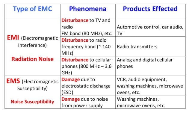
In this first blog, I’d like to look at some of the typical sources of noise. The table shown here shows the two types of Electromagnetic compatibility or EMC. EMC is defined as the ability of electronic devices to function properly in their intended electromagnetic environment.
EMC comprises two distinct types: EMI or electromagnetic interference, and EMS or electromagnetic susceptibility. EMI is generally known as radiated noise and refers to the disturbances caused by noise, whereas EMS is known as Noise Susceptibility and refers to the damage done to the system due to noise.
In the table below, you can see the different types of EMC and the typical sort of phenomena that they cause. The third column lists some typical products that can be affected by EMI and EMS, resulting in disturbance in operation or damage to the system. This list is by no means complete and is meant only to show some typical examples.

Twenty-five years ago, I was dealing with devices like those in our H8 family, which were implemented on what was then quite advanced process technology, using 1.0μm or even 0.8μm CMOS technology. Today’s devices use significantly more advanced process technology, the latest devices in our RA microcontroller family being implemented on 40 nm technology, with line widths 25 times smaller than the H8 I used to use.
As the transistor size in the latest devices becomes smaller and, probably, more importantly, the transistor switching frequency becomes faster, noise becomes an increasing factor in terms of causing a device to malfunction.

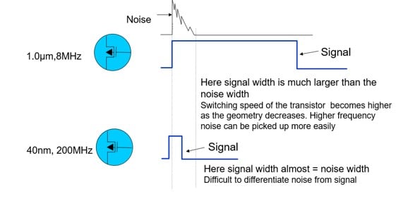
In the diagram above, you can see a simplified comparison between a device using older technology, showing transistor operation with a channel length of 1μm, with the device typically operating from what was then a fast 8 MHz Clock, with a slow transistor switching speed and the latest devices operating at up to 200 MHz or beyond, with a transistor channel length is 40 nm.
In this case, you can see that the switching time is much faster, and for the latest devices, the signal we are trying to deal with can be faster than the noise signal. Therefore, noise has become a larger concern as we move toward smaller process geometry. Renesas has taken many steps on our devices, designing them with features to help operate in such an environment, with carefully designed power supply circuits and optimized I/O buffers and specialist protection circuitry, but it’s still very important to minimize any effects in our designs as much as possible, as at the end, if noise enters the device, it’s much harder to remove.
In the next blog in this short series, we’ll look in more detail at some typical sources of noise.
Related Blogs
Reducing Noise Issues in Microcontroller Systems - Part 2
Reducing Noise Issues in Microcontroller Systems - Part 3
Reducing Noise Issues in Microcontroller Systems - Part 4
