Overview
Description
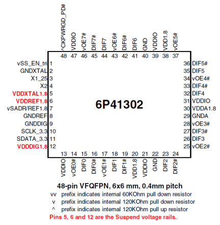
The IDT6P41302 is an 8-output very low power clock generator for PCIe Gen1-2-3 applications with integrated output terminations providing Zo=100. The device has 8 output enables for clock management and supports 2 different spread spectrum levels in addition to spread off.
Features
- 1.8V operation; reduced power consumption
- 8 - 0.7V low-power HCSL-compatible (LP-HCSL) DIF pairs w/Zo=100ohm
- 1 - 1.8V LVCMOS REF output w/Wake-On-LAN (WOL) support
- DIF cycle-to-cycle jitter <50ps
- DIF output-to-output skew <50ps
- DIF phase jitter is PCIe Gen1-2-3 compliant
- REF phase jitter is < 1.5ps RMS
- Outputs can optionally be supplied from any voltage between 1.05 and 1.8V; maximum power savings
- OE# pins; support DIF power management
- LP-HCSL differential clock outputs; reduced power and board space
- Programmable Slew rate for each output; allows tuning for various line lengths
- Programmable output amplitude; allows tuning for various application environments
- Selectable 0%, -0.25% or -0.5% spread on DIF outputs; reduces EMI
- External 25MHz crystal; supports tight ppm with 0 ppm synthesis error
- 3.3V tolerant SMBus interface works with legacy controllers
- Space saving 48-pin 6x6 mm VFQFPN; minimal board space
Comparison
Applications
Design & Development
Models
ECAD Models
Schematic symbols, PCB footprints, and 3D CAD models from SamacSys can be found by clicking on products in the Product Options table. If a symbol or model isn't available, it can be requested directly from the website.

Videos & Training
This is the first video in our PCIe series. In this video, we define PCIe architectures, focusing on common and separate clock architectures. Watch the rest of the video series below where Ron will cover the impact of different timing architectures.
Watch the Video Series Below


