Overview
Description
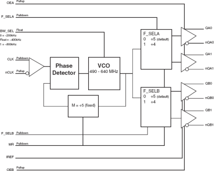
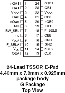
The 8741004I is a high performance Differential-to-LVDS/0.7V Differential Jitter Attenuator designed for use in PCI Express® systems. In some PCI Express systems, such as those found in desktop PCs, the PCI Express clocks are generated from a low bandwidth, high phase noise PLL frequency synthesizer. In these systems, a jitter attenuator may be required to attenuate high frequency random and deterministic jitter components from the PLL synthesizer and from the system board. The 8741004I has 3 PLL bandwidth modes: 200kHz, 600kHz and 2MHz. The 200kHz mode will provide maximum jitter attenuation, but with higher PLL tracking skew and spread spectrum modulation from the motherboard synthesizer may be attenuated. The 600kHz provides an intermediate bandwidth that can easily track triangular spread profiles, while providing good jitter attenuation. The 2MHz bandwidth provides the best tracking skew and will pass most spread profiles, but the jitter attenuation will not be as good as the lower bandwidth modes. Because some 2.5Gb SerDes have x20 multipliers while others have x25 multipliers, the 8741004I can be set for 1:1 mode or 5/4 multiplication mode (i.e. 100MHz input/125MHz output) using the F_SEL pins. The 8741004I uses Renesas' 3rd Generation FemtoClock® PLL technology to achieve the lowest possible phase noise. The device is packaged in a 24 Lead TSSOP package, making it ideal for use in space constrained applications such as PCI Express add-in cards.
Features
- Two LVDS and two 0.7V differential output pairs Bank A has two LVDS output pairs and Bank B has two 0.7V differential output pairs
- One differential clock input pair
- CLK, nCLK pair can accept the following differential input levels: LVPECL, LVDS, LVHSTL, SSTL, HCSL
- Output frequency range: 98MHz - 160MHz
- Input frequency range: 98MHz - 128MHz
- VCO range: 490MHz - 640MHz
- Cycle-to-cycle jitter: 35ps (maximum)
- Full 3.3V operating supply
- Three bandwidth modes allow the system designer to make jitter attenuation/tracking skew design trade-offs
- -40°C to 85°C ambient operating temperature
- Available in lead-free (RoHS 6) package
Comparison
Applications
Documentation
|
|
|
|
|---|---|---|
| Type | Title | Date |
| Datasheet | PDF 525 KB | |
| Overview | PDF 2.40 MB | |
| End Of Life Notice | PDF 1014 KB | |
| End Of Life Notice | PDF 537 KB | |
| Product Change Notice | PDF 567 KB | |
| End Of Life Notice | PDF 363 KB | |
| Product Change Notice | PDF 361 KB | |
| End Of Life Notice | PDF 209 KB | |
8 items
|
||
Design & Development
Models
ECAD Models
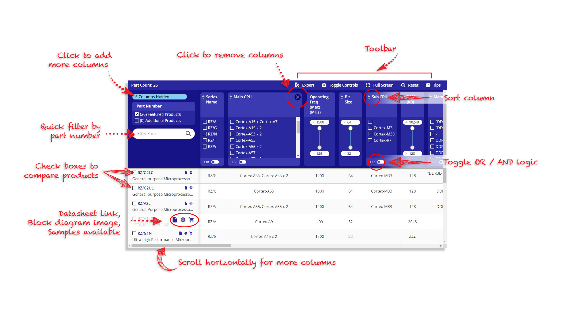
Schematic symbols, PCB footprints, and 3D CAD models from SamacSys can be found by clicking on products in the Product Options table. If a symbol or model isn't available, it can be requested directly from the website.

Videos & Training
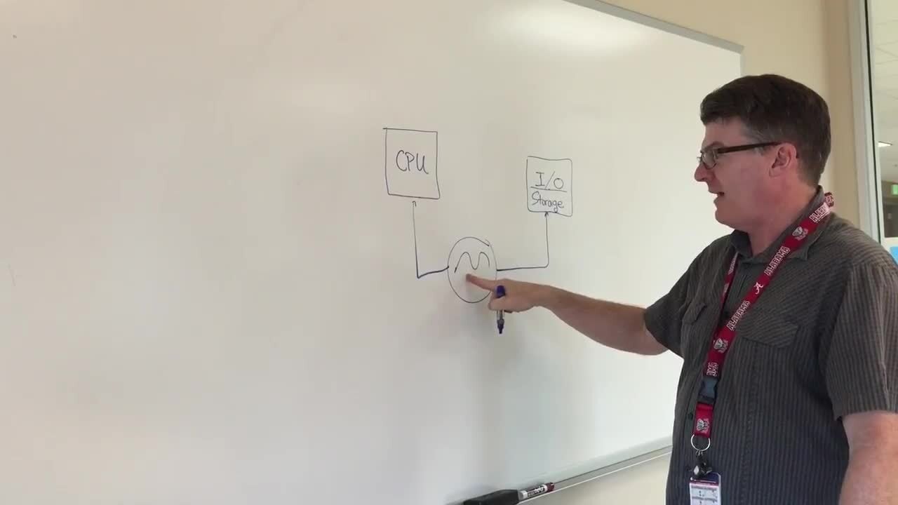
This is the first video in our PCIe series. In this video, we define PCIe architectures, focusing on common and separate clock architectures. Watch the rest of the video series below where Ron will cover the impact of different timing architectures.
Watch the Video Series Below


