Overview
Description
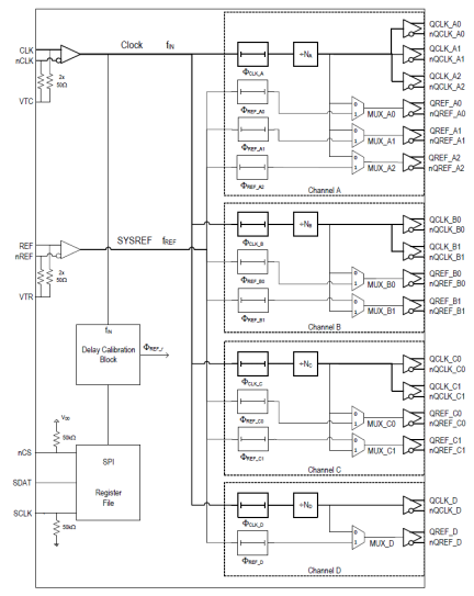
The 8V79S680 is a fully integrated, clock and SYSREF signal fanout buffer for JESD204B applications. It is designed as a high-performance clock and converter synchronization solution for wireless base station radio equipment boards with JESD204B subclass 0, 1, and 2 compliance. The main function of the device is the distribution and fanout of high-frequency clocks and low-frequency system reference signals generated by a JESB204B clock generator such as the 8V19N480, extending its fanout capabilities and providing additional phase delay. The 8V79S680 is optimized to deliver very low phase noise clocks and precise, phase-adjustable SYSREF synchronization signals as required in GSM, WCDMA, LTE, and LTE-A radio board implementations. Low-skew outputs, low device-to-device skew characteristics, and fast output rise/fall times help the system design to achieve deterministic clock and SYSREF phase relationships across devices.
The device distributes the input clock and JESD204B SYSREF signals to four fanout channels. In each channel, both input clock and SYSREF signals are fanned out to multiple clock (QCLK) and SYSREF (QREF) outputs. Clock signals can be frequency-divided in each channel. Configurable phase-delay circuits are available for both clock and SYSREF signals. The propagation delays in all signal paths are fully deterministic to support fixed phase relationships between clock and SYSREF signals within one device. The clock divider can be bypassed for low-latency clock paths. The device facilitates synchronization between frequency dividers within the device and across multiple devices, removing phase ambiguity introduced in dividers between power and configuration cycles.
Each channel supports clock frequencies up to 3GHz. In an alternative configuration, for instance, JESD204B subclass 0 and 2, the SYSREF (QREF) outputs can be configured as regular clock outputs adding additional clock fanout to the device.
All outputs are very flexible in amplitude configuration and output signal termination and allow both DC and AC coupling. Outputs can be disabled and powered down when not used. The SYSREF output pre-bias feature supports the prevention of power-on glitches and enables AC-coupling of the system synchronization signals.
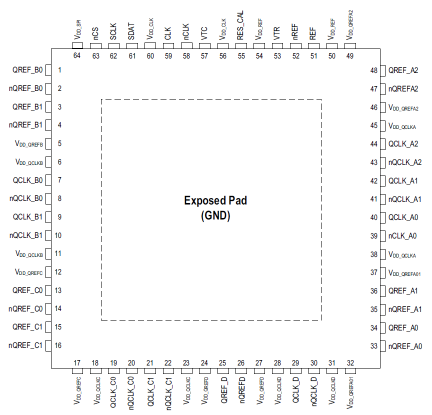
The 8V79S680 is configured through a 3-wire SPI serial interface. The device is packaged in a lead-free (RoHS 6) 64-lead VFQFN package. The extended temperature range supports wireless infrastructure, telecommunication, and networking end equipment requirements.
Features
- Supports high-speed, low-phase noise converter clocks
- Distribution, fanout, phase-delay of clock and SYSREF signals
- Very low output noise floor: -158.8dBc/Hz noise floor (245.76MHz)
- Supports clock frequencies up to 3GHz, including clock output frequencies of 983.04MHz, 491.52MHz, 245.76MHz, and 122.88MHz
- 4 output channels with a total of 16 differential outputs, organized in:
- 8 dedicated clock outputs
- 8 outputs configurable as SYSREF outputs with individual phase delay stages, or configurable as additional clock outputs
- Each channel contains:
- Frequency dividers: ÷1, ÷2, ÷4, ÷6, ÷8, ÷12, ÷16
- Clock phase delay circuits
- Clock phase delay circuits:
- Clock: Delay unit is the clock period; 256 steps
- SYSREF: Configurable precision phase delay circuits: 8 steps of 131ps, 262ps, 393ps, or 524ps
- Flexible differential outputs:
- LVDS/LVPECL configurable
- Amplitude configurable
- Power-down modes for unused outputs
- Supports DC and AC coupling
- QREF (SYSREF) output pre-bias feature to prevent glitches when turning output on or off
- Supply voltage:
- 3.3V core and signal I/O
- 1.8V digital control SPI I/O (3.3V-tolerant inputs)
- 64 VFQFN-P package (9mm x 9mm x 0.85mm)
- Ambient temperature range: -40 °C to +85 °C
Comparison
Applications
Documentation
|
|
|
|
|---|---|---|
| Type | Title | Date |
| Datasheet | PDF 940 KB | |
| Manual - Hardware | PDF 2.51 MB | |
| Product Change Notice | PDF 1.26 MB | |
| Overview | PDF 331 KB | |
| Application Note | PDF 601 KB | |
| Application Note | PDF 586 KB | |
| Product Change Notice | PDF 983 KB | |
7 items
|
||
Design & Development
Models
ECAD Models
Schematic symbols, PCB footprints, and 3D CAD models from SamacSys can be found by clicking on products in the Product Options table. If a symbol or model isn't available, it can be requested directly from the website.

Product Options
Applied Filters:

