Overview
Description
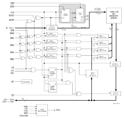
The 71V35761 3.3V CMOS SRAM is organized as 128K x 36. It contains write, data, address and control registers. The burst mode feature offers the highest level of performance to the system designer, as the 71V35761 can provide four cycles of data for a single address presented to the SRAM.
Features
- High system speed 200MHz (3.1ns clock access time)
- LBO input selects interleaved or linear burst mode
- Self-timed write cycle with global write control (GW), byte write
- enable (BWE), and byte writes (BWx)
- 3.3V core power supply
- Power down controlled by ZZ input
- 3.3V I/O
- Optional - Boundary Scan JTAG Interface (IEEE 1149.1
- compliant)
- Available in 100-pin TQFP, 119-pin BGA and 165 fpBGA packages
Comparison
Applications
Design & Development
Models
ECAD Models
Schematic symbols, PCB footprints, and 3D CAD models from SamacSys can be found by clicking on products in the Product Options table. If a symbol or model isn't available, it can be requested directly from the website.

Product Options
Applied Filters:
