Overview
Description
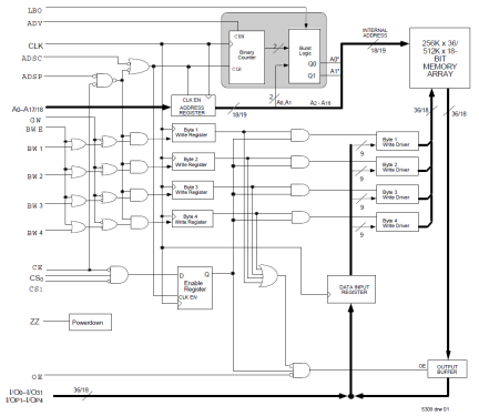
The 71V67703 3.3V CMOS SRAM is organized as 256K x 36. The 71V67703 SRAM contains write, data, address and control registers. There are no registers in the data output path (flow-through architecture). The burst mode feature offers the highest level of performance to the system designer, as it can provide four cycles of data for a single address presented to the SRAM.
Features
- Fast access times 7.5ns up to 117MHz clock frequency
- LBO input selects interleaved or linear burst mode
- Self-timed write cycle with global write control (GW), byte write
- enable (BWE), and byte writes (BWx)
- 3.3V core power supply
- Power down controlled by ZZ input
- 3.3V I/O supply (VDDQ)
- Available in 100-pin TQFP, 119-pin BGA and 165 fpBGA packages
Comparison
Applications
Design & Development
Models
ECAD Models
Schematic symbols, PCB footprints, and 3D CAD models from SamacSys can be found by clicking on products in the Product Options table. If a symbol or model isn't available, it can be requested directly from the website.


