Overview
Description
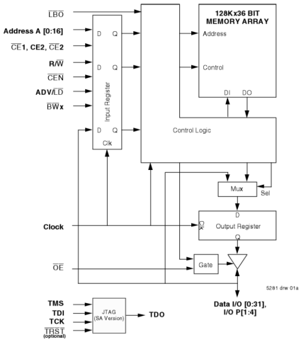
The 71V3556 3.3V CMOS synchronous SRAM, organized as 128K x 36, is designed to eliminate dead bus cycles when turning the bus around between reads and writes or writes and reads. Thus, it has been given the name ZBT™, or Zero Bus Turnaround. The 71V3556 contains data I/O, address, and control signal registers.
Features
- High-performance system speed 200MHz (x18) (3.2ns Clock-to-Data access)
- ZBT feature - No dead cycles between write and read cycles
- Internally synchronized output buffer enable eliminates the need to control OE
- Single R/W (Read/Write) control pin
- Positive clock-edge triggered address, data, and control signal registers for fully pipelined applications
- 4-word burst capability (interleaved or linear)
- Individual byte write (BW1 - BW4) control (May tie active)
- Three chip enables for simple depth expansion
- 3.3V power supply (±5%), 3.3V I/O supply (VDDQ)
- Optional- Boundary Scan JTAG interface (IEEE 1149.1 compliant)
- Available in 100-pin TQFP, 119-pin BGA, and 165 fpBGA packages
Comparison
Applications
Design & Development
Models
ECAD Models
Schematic symbols, PCB footprints, and 3D CAD models from SamacSys can be found by clicking on products in the Product Options table. If a symbol or model isn't available, it can be requested directly from the website.

Product Options
Applied Filters:
