Overview
Description
Support is limited to customers who have already adopted these products.
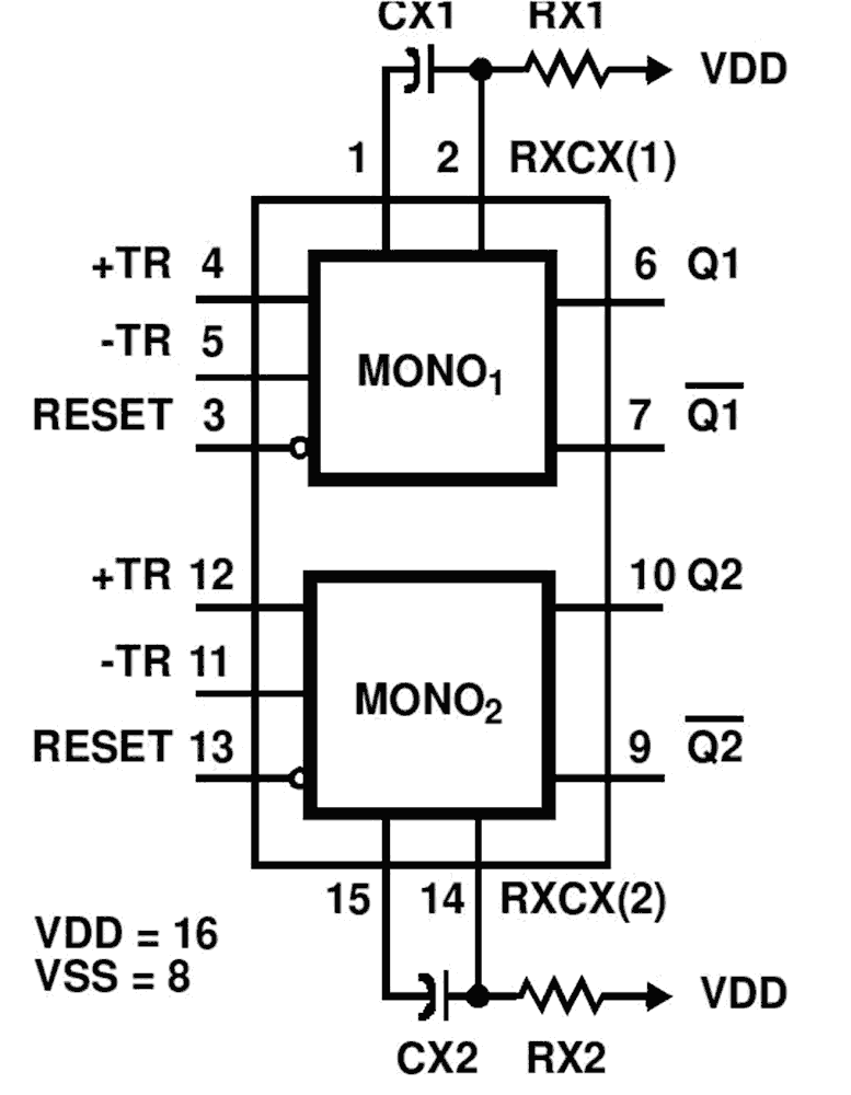
CD14538BMS dual precision monostable multivibrator provides stable retriggerable/ resettable one-shot operation for any fixed-voltage timing application. An external resistor (RX) and an external capacitor (CX) control the timing and accuracy for the circuit. Adjustment of RX and CX provides a wide range of output pulse widths from the Q and Q terminals. The time delay from trigger input to output transition (trigger propagation delay) and the time delay from reset input to output transition (reset propagation delay) are independent of RX and CX. Precision control of output pulse widths is achieved through linear CMOS techniques. Leading-edge-triggering (+TR) and trailing-edge-triggering (-TR) inputs are provided for triggering from either edge of an input pulse. An unused +TR input should be tied to VSS. An unused -TR input should be tied to VDD. A RESET (on low level) is provided for immediate termination of the output pulse or to prevent output pulses when power is turned on. An unused RESET input should be tied to VDD. However, if an entire section of the CD14538BMS is not used, its inputs must be tied to either VDD or VSS. See Table 1. In normal operation the circuit retriggers (extends the output pulse one period) on the application of each new trigger pulse. For operation in the non-retriggerable mode, Q is connected to -TR when leading-edge triggering (+TR) is used or Q is connected to +TR when trailing-edge triggering (-TR) is used. The time period (T) for this multivibrator can be calculated by: T = RXCX. The minimum value of external resistance, RX is 4KΩ. The minimum and maximum values of external capacitance, CX, are 0pF and 100µF, respectively. The CD14538BMS is interchangeable with type MC14538 and is similar to and pin-compatible with the CD4098B* and CD4538B**. * T = 0. 5 RXCX for CX ≥ 1000pF. * T = RX CX; CX min = 5000pF. The CD14538BMS is supplied in these 16-lead outline packages: Braze Seal DIP H4X Frit Seal DIP H1L Ceramic Flatpack H6W
Features
- High-Voltage Type (20V Rating)
- Retriggerable/Resettable Capability
- Trigger and Reset Propagation Delays Independent of RX, CX
- Triggering From Leading or Trailing Edge
- Q and Q Buffered Outputs Available
- Separate Resets
- Wide Range of Output-Pulse Widths
- Schmitt-Trigger Input Allows Unlimited Rise and Fall Times On +TR and -TR Inputs
- 100% Tested For Maximum Quiescent Current at 20V
- Maximum Input Current of 1µA at 18V Over Full Package-Temperature Range:
- 100nA at 18V and +25°C
- Noise Margin (Full Package-Temperature Range):
- 1V at VDD = 5V
- 2V at VDD = 10V
- 2.5V at VDD = 15V
- 5V, 10V and 15V Parametric Ratings
- Standardized Symmetrical Output Characteristics
- Meets All Requirements of JEDEC Tentative Standards No. 13B, "Standard Specifications for Description of "B" Series CMOS Devices
Comparison
Applications
- Pulse Delay and Timing
- Pulse Shaping
Documentation
Featured Documentation
Log in required to subscribe
|
|
|
|
|---|---|---|
| Type | Title | Date |
| Datasheet | PDF 572 KB | |
| Brochure | PDF 5.02 MB | |
| Brochure | PDF 467 KB | |
| White Paper | PDF 533 KB | |
| Product Advisory | PDF 499 KB | |
| Product Change Notice | PDF 230 KB | |
| Application Note | PDF 338 KB | |
7 items
|
||
Design & Development
Models
ECAD Models
Schematic symbols, PCB footprints, and 3D CAD models from SamacSys can be found by clicking on products in the Product Options table. If a symbol or model isn't available, it can be requested directly from the website.

Processing table
| SBDIP | 16 | Tube | 20.3 x 7.5 x 2.41 | No | 15 | -55 to +125°C | |||
| CFP | 16 | Tray | 10.4 x 6.9 x 0.00 | No | 15 | -55 to +125°C |
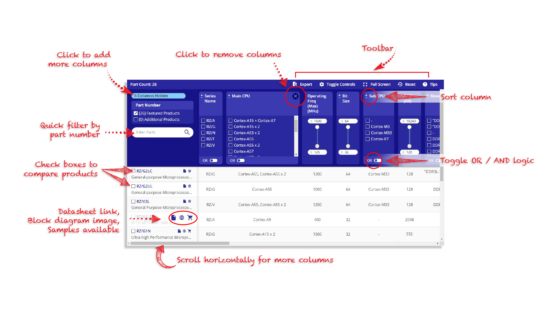
Tips for Using This Parametric Table:
- Hide Filters button in header: Collapse or expands filters
- Column sort buttons in header: Sort Column alphabetically / numerically descending or ascending
- Reset button in header: Reset all filters to the page default
- Full Screen button in header: Expand the table to full screen view (user must close out of full screen before they can interact with rest of page)
- Export button in header: Export the filtered results of the table to an Excel document
- Filter parts search bar in header: Type to filter table results by part number
- Hide column button in column headers: Select to hide columns in table
- AND / OR toggle switches in header: Toggles the logic of this particular filter to be “AND” or “OR” logic for filtering results
- Multiselect checkboxes at beginning of each row in table: Select these checkboxes to compare products against each other
- Document icon next to product name in row: View the featured document for this product
- Chip icon next to the right of the document icon in row: View the block diagram for this product
- Cart icon to the right of the chip icon: Indicates that samples are available for this product