Overview
Description
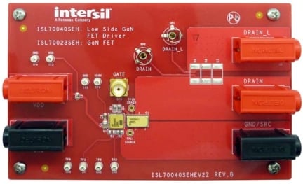
The ISL70040SEHEV2Z evaluation platform evaluates the ISL70040SEH alongside the ISL70023SEH. The same board can be used to evaluate the ISL73040SEH alongside the ISL73023SEH, which are the same die offered with different radiation assurance screening.
The ISL70040SEH is designed to drive enhancement mode Gallium Nitride (GaN) FETs in isolated topologies and boost type configurations. It operates across a supply range of 4.5V to 13.2V and offers both non-inverting and inverting inputs to satisfy non-inverting and inverting gate drive within a single device.
The ISL70040SEH has a 4.5V gate drive voltage (VDRV) that is generated using an internal regulator which prevents the gate voltage from exceeding the maximum gate-source rating of enhancement mode GaN FETs. The gate drive voltage also features an undervoltage lockout (UVLO) protection that ignores the inputs (IN/INB) and keeps OUTL turned on to ensure the GaN FET is in an OFF state whenever VDRV is below the UVLO threshold. The ISL70040SEH inputs can withstand voltages up to 14.7V regardless of the VDD voltage. This allows the ISL70040SEH inputs to be connected directly to most PWM controllers. The split outputs of the ISL70040SEH offer the flexibility to adjust the turn-on and turn-off speed independently by adding additional impedance to the turn-on/off paths.
The ISL70023SEH is a 100V N-channel enhancement mode GaN power transistor. GaN’s exceptionally high electron mobility and low temperature coefficient allows for very low r DS(ON), while its lateral device structure and majority carrier diode provide exceptionally low QG and zero QRR. The end result is a device that can operate at a higher switching frequency with more efficiency while reducing the overall solution size.
Features
- Wide VDD range single
- 4.5V to 13.2V
- Location provided for load resistors to switch the GaN FET with a load
- SMA connector on the gate drive voltage to analyze the gate waveforms
- Drain/Source sense test points to analyze the drain to source waveforms
- Banana jack connectors for power supplies and drain/source connections
Applications
- Switching regulation
- Motor drives
- Relay drives
- Inrush protection
- Down hole drilling
- High reliability industrial
- Flyback and forward converters
- Boost and PFC converters
- Secondary synchronous FET drivers
Documentation
|
|
|
|
|---|---|---|
| Type | Title | Date |
| Manual - Development Tools | PDF 1.74 MB | |
| Datasheet | PDF 521 KB | |
| Report | PDF 433 KB | |
| Report | PDF 368 KB | |
| Datasheet | PDF 1.08 MB | |
| Report | PDF 251 KB | |
6 items
|
||
Design & Development
Software & Tools
Videos & Training
Renesas, a leading solution provider in the satellite and high reliability industry, discusses a technology leap into Gallium Nitride with its family of Intersil GaN products. The ISL70024SEH is designed from the ground up with space applications in mind to provide steady and reliable performance when exposed to total ionizing dose (TID) or heavy ions. The Intersil GaN driver and FET together allow more efficient switching, higher frequency operation, reduced gate drive voltage and a smaller solution size compared to their traditional silicon counterparts.
Transcript
Renesas is a leading solution provider in the satellite and high reliability industry, and is now introducing a technology leap into Gallium Nitride with its new family of GaN products.
GaN is a wideband gap material and compared to silicon, the drain to source distance can be a factor of ten smaller which translates to a much smaller RDS(on). While silicon FETs are very close to their theoretical limit of channel length, GaN has much more room for improvement. GaN's advantages to the power supply designers include size, weight and efficiency.
The size and weight reduction of using GaN over silicon comes from two factors. The first is that heat-sinking requirements are not as much due to GaN's reduced parasitics. And the second, is the use of smaller output filters due to being able to switch at higher frequencies. This allows GaN to achieve excellent efficiencies at a compact solution size.
Another plus point, when it comes to ionizing radiation in contrast to silicon FETs, GaN FETS do not have a gate oxide layer. That means radiation cannot form traps in the gate oxide that would otherwise shift the gate to source threshold voltage.
As you can see in the graph, the current technology of GaN is already orders of magnitude better and figure of merit, and this will only get better with time. To be able to take full advantage of GaN FETs, you'll need a good gate driver to go with it. So Renesas is now introducing the industry's first radiation hardened low-side GaN FET driver.
A GaN FET gate driver needs to provide a well-regulated gate voltage that never exceeds 6V under all conditions. The ISL70040SEH regulates a 4.5V gate driver in order to meet the voltage margins of the space and high reliability industry.
Here we have the ISL70040SEH low-side driver and the ISL70024SEH, the 200V GaN FET, in action. The VDD is set to 5V and the inputs are driven with a function generator set to a frequency of 500kHz. As you can see, it has fast transition times with minimal overshoot on the rising and falling edges with a well-regulated 4.5V gate drive voltage.
It is designed from the ground up with space applications in mind to provide steady and reliable performance when exposed to total ionizing dose (TID) or heavy ions. This first graph shows minimal shift in V drive, the gate drive voltage across TID for both high dose rate and low dose rate. The next graph shows how steady the operating supply current is across TID. For both gate drive voltage and supply current, we are well within the spec limits. From a single event transient perspective, at an LET limit of 86MeV, the ISL70040SEH had a very small cross section of ≤1.7 x 10⁻⁶cm2 for dynamic switching, and had no SETs for static input, high or low.
GaN FETS are a very good fit for satellite applications but require a good gate driver to realize their full potential. Together they allow more efficient switching, higher frequency operation, reduced gate drive voltage and a smaller solution size compared to their traditional silicon counterparts.
For more information, datasheets, TID/SEE test reports, or to order parts or evaluation boards, please visit our Rad Hard GaN FET product page.


