As the demand grows for higher functionality and intelligence at the edge and endpoint, so does the need for greater processing power and larger memory in these devices. Applications are more feature-rich and users demand higher levels of functionality built into their products, including sophisticated graphics and user interfaces, learning algorithms, network connectivity, and advanced security. More recently, machine learning has enabled voice and vision AI capabilities that help devices make intelligent decisions at the edge and trigger actions without human intervention. Sophisticated software frameworks are an essential part of these solutions.
While processing power is key for all these kinds of applications, they also drive the need for fast, reliable, low-power, and non-volatile storage for code and data. When developing embedded systems, the memory choices designers make can significantly impact performance, cost, design complexity, and power consumption. New architectures are needed to address the evolving requirements for higher performance, larger memory, and lower power, all while keeping costs low. Close collaboration with memory manufacturers is required to ensure fully verified solutions that meet the performance requirements. Let’s take a look at the various memory architecture options and the optimal use cases for them.
Internal Flash or External Memory
Traditionally, general-purpose MCUs used in low to mid-range performance applications incorporate embedded flash (typically < 2MB) as the non-volatile storage of choice for code. These integrated MCUs are very well-suited for most low to mid-range IoT applications in diverse market segments such as industrial or building automation, medical, home appliances, or smart homes. Embedded flash has a number of advantages – lower latency, lower power, and higher performance – and provides a more integrated solution suited for simpler, space-constrained applications and reduced design complexity. From a security point of view, it eliminates an additional attack surface. So MCUs with integrated embedded flash are still the preferred solution for most applications with lower performance and functionality needs.
But embedded flash memory comes at a cost and beyond a certain memory density (like 2MB), starts to become cost-prohibitive. Embedded flash is expensive and increases the complexity and costs of MCU wafer processing. The additional manufacturing steps needed to embed flash significantly increase the cost of silicon.
Additionally, MCU manufacturers are increasingly moving to more advanced, finer process geometries, like 28/22nm or lower, in order to scale to much higher performance and integrate more functionality on-chip. It is now typical to see MCUs with speeds in the range of 400MHz to 1GHz with support for advanced graphics, analog, connectivity plus safety features, and advanced security to protect against data/IP theft and tampering. While this addresses the performance needs, embedding memory on these devices becomes a challenge as embedded flash does not scale well at lower process geometries and the flash cell does not shrink efficiently below 40nm. All this makes it less feasible or more expensive at the lower process geometries.
External Memory
Designers are considering new architectures to close this gap and are increasingly moving towards using external flash for their more demanding, higher-performance applications. The support for more complex use cases such as high-end graphics, audio processing, or machine learning drives this need, and a sharp decrease in standalone memory pricing fuels this trend. Using external memory enables the expansion of code and data space in an embedded system, as the external flash is basically a part of the MCU memory map that can be read directly and used for data logging or software storage and execution.
For IoT product manufacturers, moving to external flash for their high-performance applications provides several advantages, including offering flexibility in memory size selection and future-proofing their designs. As developers add more functionality requiring a larger memory footprint, it is a fairly simple exercise to swap out a smaller-sized memory with a pin-compatible, larger option. It also allows them to take a unified platform approach for their various designs.
Of course, there are downsides, such as the additional latency involved in accessing external memory (mitigated with Quad/Octal memories and careful use of caches), slightly higher power, and the additional cost for external memory. It also increases board design complexity and requires additional routing on the PCB and attention to signal integrity.
For MCU manufacturers, separating the MCU from the memory allows them to move to more advanced process nodes for higher performance, higher functionality, and power efficiency, and to lower their device costs. Most manufacturers now incorporate Quad or Octal SPI interfaces with support for Execute-in-Place (XiP) capability that allows for seamless interface with these NOR flash devices. Some MCUs support Decryption-On-the-Fly (DOTF) which allows an encrypted image to be stored in external flash and brought in securely for execution. This solution provides the high performance, low power, and advanced security required for today's edge applications.

Challenges with External Memory and Mitigation
Of course, there are challenges with external memory, including concerns around the latency associated with external flash and its impact on overall performance. It is possible to mitigate this bandwidth limitation somewhat by using either a Quad or Octal SPI interface that allows data to be transferred over four or eight parallel lines vs. the single line with a regular SPI. With Double Data Rate (DDR), this throughput can be doubled by sending data on both the rising and falling edge of the clock. External flash manufacturers also build in support for burst read modes for faster access to data and caching can be used to mitigate some of the latency effects, but careful management of software is required to make optimal use of the caches. System designers can also alleviate some latency concerns by transferring the code to internal SRAM and executing out of SRAM for the highest performance.
There are also concerns about higher power consumption associated with using an external flash, so memory manufacturers pay special attention to optimizing the current consumption of these devices. There is some security risk associated with external memory, as it adds an additional attack surface, creating a vulnerability that can be exploited by hackers and needs to be protected. This requires MCU manufacturers to add encryption/decryption capability to the Quad/Octal SPI interface so that encrypted code can be stored and brought in securely.
Using External Flash with RA MCUs
Renesas' RA family of MCUs integrates embedded flash as well as multiple memory interfaces to external memory, to provide maximum flexibility and performance. They support either Quad or Octal SPI interfaces for higher data throughput by using four or eight data lines instead of the usual one with the SPI interface. This can significantly enhance the performance, especially in applications that require fast memory accesses such as graphics, audio, or data logging.
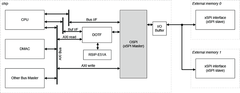
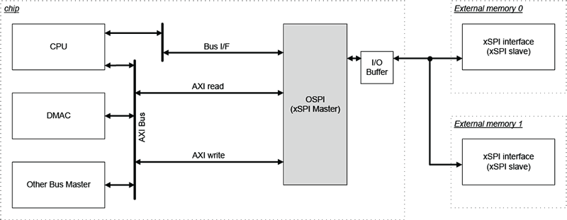
All of the RA8 Series MCUs include an eXpanded Serial Peripheral Interface (xSPI) compliant Octal SPI interface. The xSPI protocol specifies the interface to non-volatile memory devices and enables high data throughput, low signal count, and limited backward compatibility with legacy SPI devices. Two external memory devices can be connected to the Octal SPI interface using chip selects, as shown below, allowing designers greater flexibility. Some RA8 MCUs also support Decryption-On-the-Fly (DOTF) which allows encrypted images stored in external flash to be brought in securely for execution. Figures 2 and 3 show the Octal SPI interface on the RA8 MCUs, with and without DOTF.


Some features of the Octal SPI interface:
- Protocol – xSPI, compliant with
- JEDEC standards JESD251 (Profile 1.0 and 2.0)
- JESD251-1 and JESD252
- Memory types supported – Octal flash and Octal RAM, HyperFlash and HyperRAM
- Data throughput – Up to 200Mbytes per second
- Data transmission/reception – Can communicate with up to 2 slaves using chip select, not concurrent
- Supports Execute-in-Place (XiP) operation
- Supported modes
- 1/4/8-pin with SDR/DDR (1S-1S-1S, 4S-4D-4D, 8D-8D-8D)
- 2/4-pin with SDR (1S-2S-2S, 2S-2S-2S, 1S-4S-4S, 4S-4S-4S)
- Memory mapping
- Supports up to 256MB address space each CS
- Prefetch function for burst-read with low latency
- Outstanding buffer for burst-write with high throughput
- Security – Support for DOTF (available on some RA8 MCUs)
In addition to internal flash and external memory interfaces, the RA8 MCUs also include Tightly Coupled Memory (TCM) and I/D caches that can help in optimizing performance. The TCM is zero wait-state memory and has the lowest latency of all the on-chip memory; it can be used for the most critical portions of the code.
Multiple flexible memory configurations are possible using various memories and memory interfaces available on the RA8 Series MCUs. Code can be stored in and executed from internal embedded flash, enabling a simple, low latency, highly secure, and power-efficient system. However, this is not a scalable solution and any increase in code size beyond the size of embedded flash will need to be addressed with external memory.
In the second configuration, code is stored in and executed out of external flash. This is the XiP capability and is the most flexible and scalable option. The external memory can simply be swapped out for a pin-compatible, larger-density device as code size grows, enabling easy upgrades without having to re-design boards. This comes at the cost of slightly higher power consumption and larger latency that could have an impact on overall performance.
Code can also be stored in external flash and brought into internal SRAM or TCM for execution. This provides the highest performance because code is executed out of fast SRAM, but there is a limitation to code size based on SRAM size and increased software complexity if code size exceeds available SRAM or TCM. Wakeup times could also increase since code lost when the SRAM is shut down, would need to be reloaded on each power cycle.
Conclusion
There is no single correct answer when it comes to memory option selection. While most low to mid-end IoT applications can use internal flash, many higher-performance applications demand the use of external flash. Memory selection must be based on several considerations – application requirements, memory size needed, performance expected, system architecture, power consumption targets, security concerns, and future product/platform plans, among others.
Both options addressed have benefits and drawbacks:
Internal flash
- Provides simplicity
- Tightly integrated
- Highly secure solution
- Suitable for a broad range of applications
External flash
- Flexibility
- Memory expansion
- Scalability
- Ideal for emerging IoT and Edge AI applications
By understanding these trade-offs, developers can make informed decisions aligned with their project goals.
Get all of the details on the flexible memory options available on the RA8 MCU Series on each device product page, along with datasheets, samples, and evaluation kits.
