Overview
Description
The 9DBV0231 very-low power, 2-output, 1.8V, PCIe zero-delay/fanout clock buffer has two output enables for clock management.

Features
- LP-HCSL outputs; save 4 resistors compared to standard HCSL outputs
- 35mW typical power consumption in PLL mode; minimal power consumption
- Spread Spectrum (SS) compatible; allows use of SS for EMI reduction
- OE# pins; support DIF power management
- HCSL-compatible differential input; can be driven by common clock sources
- SMBus-selectable features; optimize signal integrity to application
- Slew rate for each output
- Differential output amplitude
- Pin/Software selectable PLL bandwidth and PLL bypass; minimize phase jitter for each application
- Outputs are blocked until PLL is locked; clean system start-up
- Device contains default configuration; SMBus interface is not required for device control
- 3.3V tolerant SMBus interface works with legacy controllers
- Space-saving 24-pin 4mm x 4mm VFQFPN; minimal board space
Comparison
Applications
1.8V PCIe Gen 1–5 Zero-Delay/Fanout Buffer (ZDB/FOB)
Design & Development
Models
ECAD Models
Schematic symbols, PCB footprints, and 3D CAD models from SamacSys can be found by clicking on products in the Product Options table. If a symbol or model isn't available, it can be requested directly from the website.

Product Options
Applied Filters:
Videos & Training
PCI Express (PCIe) Clock Overview by IDT
A detailed overview of IDT's full-featured PCI Express (PCIe) clock and timing solutions. The presentation addresses PCIe Gen 1, Gen 2, Gen 3, and Gen 4 architectures and how IDT's industry-leading solutions provide all the functions, features, and performance required by the application.
Presented by Ron Wade, System Architect at IDT. For more information visit the PCIe clocks page.
TRANSCRIPT
Hi there. This is the first in the five-part series on IDT's new full-featured PCIe clock family. The first part in the series will be a family overview. There will also be a part on the clock generators, another section covering the clock buffers, a fourth section that will deal with the clock multiplexers and finally, a fifth section covering some of the applications for the full-featured PCIe clocks. So let's jump right into the family overview.
So PCI Express is evolving. There are two major things happening in PCI Express these days. One is the PCIe Gen4 specification is moving toward 0.9 drafts stage. And Gen4 is going to bring 16 Gbps data transfers to the architecture or to the PCI Express world. And then there's also going to be two new architectures which are supported in a non-specific way. The two architectures are the separate reference no spread--or SRNS--and the separate reference independence spread--or SRIS--clock architectures. These are going to be supported in the PCI Express Gen4 specification but there will be no explicit specifications on the reference clocks. So what the phrase is, is that SRNS and SRIS clocking will be implementation dependent. And what that means is that there's not gonna be an explicit reference clock jitter specification. And that means that IDT will need to work with the SOC vendors to ensure interoperability. And regardless of whether there's an explicit specification or not, IDT delivers solutions for these architectures and increasing performance requirements and we have always done so.
So in terms of the IDT's PCIe clock families, there are three major families. The focus of these series of presentations is on the full-featured PCIe, which you see on the left of your screen. We've just introduced the new L-series parts to production, which are the 3.3V devices that have the best performance - PCI Gen1 through 4, and also SRNS and SRIS support. And those follow the very successful 1.8V V-series and the 1.5V U-series parts which have been in the market for a couple of years supporting Gen1 through 3. The other specs and the Gen4 common clock spec are being evaluated against these parts to see if they will be able to do Gen4 or not. And so those other specs are TBD. The other family that we have is the PhiClock family, which is PhiClock plus PCIe in this case, where we add some less than 300 femtosecond RMS high-performance SerDes clocks or PhiClocks and then also provide some PCI Express Gen1 through 4 clocks.
Then the last family is when you really need to go smaller and you don't need all the features, you want a simpler board layout and you have very tight space constraints, is the micro-PCIe family which will be the subject of another presentation. And we're defining smaller as in micro-PCIe as any device that is in a 3x3 millimeter or smaller package.
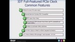
So the common features of IDT's full-featured PCIe family are as follows. You have an Output Enable pin for every PCIe clock, you have Spread Spectrum Clocking capability and compatibility across every part in the family. On the clock generators, there is a reference output which can save you an XO in your system. And then to make it really simple to use the parts, you have--on the clock generators--you have pin control of three different spread amounts including spread off. And you also have on the zero-delay buffers pin control of the PLL bandwidth, whether you want it to be high bandwidth, low bandwidth or the PLL bypassed, that is all done from a single pin.
The other common feature is multiple, pin selectable SMBus addresses. So the clock generators have a choice of two SMBus addresses, the buffers have a choice of three SMBus addresses and those five addresses do not overlap. So you can have up to five of these devices on a single SMBus segment. The other common feature is that we use low power, and some people refer to this as push-pull, but we use low-power HCSL outputs on all the parts and they are offered with a choice of 100 ohm integrated terminations or 85 ohm integrated terminations. And all the parts in the full-featured family are between 2.5 mm x 2.5 mm up to 6 mm x 6 m. They all offer I-temp operation and the most power consuming part consumes 211 mW, so they are very power efficient.
So, the 3.3V full-featured PCIe clock family, which is the newest one, provides the basic functions you need for clocking, provides a clock generator function, provides both zero delay and fanout buffers, and provides a clock muxing function. And the muxes are two inputs with different numbers of outputs. In the 3.3V family, it's a 2-input and 4-output mux.
So the family has performance. The 3.3V family is PCIe Gen1, 2, 3, 4 common clocked compliant. It also supports the SRNS and SRIS architectures. You've got flexibility in the family where you can right-size the part for your design because we provide from two to nine outputs. Again, the 3.3V family does allow factory OTP customization if you have a particular setting that you would like to adjust, whether it's slew rate, output impedance, polarity of control signals, or even on the clock generators, maybe you prefer to run from a 20 MHz or 24 MHz reference clock instead of 25. That can easily be OTP into the parts.
We also have easy AC coupling to other logic standards such LVPECL, LVDS, and CML. There's SMBus programmability for the signal integrity and functionality. And again that can be OTP customized for your particular needs. And then we have 1.5 and 1.8V versions of the parts available for the more power-conscious applications that might be out there. As far as 3.3V size and power, this family ranges from a 4x4 mm at the smallest end to a 6x6 mm QFN in the largest part. These save up to 53% board area compared to IDT's legacy 3.3V current mode devices such as the 9DB803 for instance.
The integrated terminations allow you to save up to 36 resistors and that 36 resistors represent 62 mm2 of board area. So really great for space constrained designs. And then power-wise, the low power HCSL outputs allow up to an 80% power savings with the 3.3V parts. If you can use 1.5 or 1.8 in your design you can save even more power. The parts are easy to use because as shown earlier, the basic functions are controlled by hardware pins. So you do not need to use the SMBus for most applications. And we do have the individual OE pin on each PCIe output.
So the 3.3V full-featured PCIe clocks support Gen1, 2, 3, 4 common clock, SRIS and SRNS. It is a family of parts with a clock generator, fanout buffers, zero delay buffers, and clock multiplexers. And it supports both 100 ohm environments and 85 ohm environments without any external components. The numbering scheme is really easy. All parts start with a 9. And if you're looking for a generator it's a 9FG, the FG stands for frequency generator actually. If you're looking for a buffer, it's 9DB, for differential buffer. And if you're looking for a mux, it's 9DM, for differential mux. And then the operating voltage is the fourth character in the part number, L is for 3.3V, which stands for Low power. The V indicates 1.8V, or Very low power. And then the U indicates 1.5V, or Ultra-Low power.
The next two digits then provide the number of PCIe clock output pairs. So arranging from 1 all the way up to 9 currently. So that's the number of outputs. And then finally, the next to last digit indicates the output impedance. So a 33-ohm output impedance would have a 3 as the next to last digit. And then the device variant would be like 31, 32, 33, 34, etc. 100ohm output impedance has the next to last digit as a 4. And you would have 41, 42, 43, 44, etc. And then finally the 85-ohm output impedance starts with a 5 and that would be like 51, 52, 53, etc. That's it for the PCI Express family overview. Thank you for watching.
Video List