Overview
Description
The 9EX21531 provides 15 output clocks for PCIe Gen1/ 2/3 applications. The 9EX21531 has 4 selectable SMBus addresses, and dedicated CKPWRGD/PD# and VDDA pins for easy board design. A differential clock from a CK410B+ or CK420BQ main clock generator, such as the 932S421, drives the 9EX21531. In fanout mode, the 9EX21531 provides outputs up to 166MHz.


Features
- 15 - 0.7V current mode differential HSCL output pairs
- Pin compatible to 9EX21501/ Easy PCIe Gen3 upgrade
- 4 Selectable SMBus Addresses/Multiple devices can share the same SMBus Segment
- 8 dedicated and 2 group OE# pins/Hardware control of the outputs
- PLL or bypass mode/PLL can dejitter incoming clock
- Selectable PLL bandwidth/minimizes jitter peaking in downstream PLL's
- Spread Spectrum Compatible/tracks spreading input clock for low EMI
- SMBus Interface/unused outputs can be disabled
- Undriven differential outputs in Power Down mode/ Easy power management
- Cycle-to-cycle jitter <50ps
- Output-to-output skew < 150 ps
- PCIe Gen3 phase jitter < 1.0ps RMS
Comparison
Applications
Design & Development
Models
ECAD Models
Schematic symbols, PCB footprints, and 3D CAD models from SamacSys can be found by clicking on products in the Product Options table. If a symbol or model isn't available, it can be requested directly from the website.

Processing table
| VFQFPN | 64 | Tray | 3 | 0 | 207 | Yes | e3 Sn | 0 to 70°C | ||
| VFQFPN | 64 | Reel | 3 | 3000 | 0 | Yes | e3 Sn | 0 to 70°C |
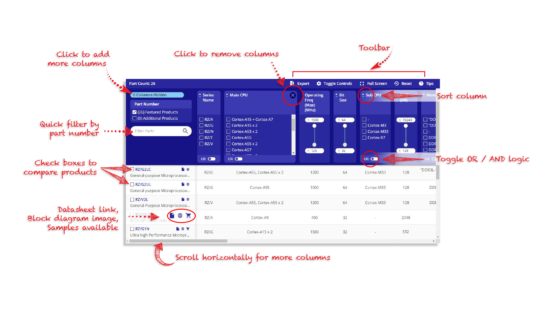
Tips for Using This Parametric Table:
- Hide Filters button in header: Collapse or expands filters
- Column sort buttons in header: Sort Column alphabetically / numerically descending or ascending
- Reset button in header: Reset all filters to the page default
- Full Screen button in header: Expand the table to full screen view (user must close out of full screen before they can interact with rest of page)
- Export button in header: Export the filtered results of the table to an Excel document
- Filter parts search bar in header: Type to filter table results by part number
- Hide column button in column headers: Select to hide columns in table
- AND / OR toggle switches in header: Toggles the logic of this particular filter to be “AND” or “OR” logic for filtering results
- Multiselect checkboxes at beginning of each row in table: Select these checkboxes to compare products against each other
- Document icon next to product name in row: View the featured document for this product
- Chip icon next to the right of the document icon in row: View the block diagram for this product
- Cart icon to the right of the chip icon: Indicates that samples are available for this product
Videos & Training
PCIe Clocking Architectures (Common and Separate)
This is the first video in our PCIe series. In this video, we define PCIe architectures, focusing on common and separate clock architectures. Watch the rest of the video series below where Ron will cover the impact of different timing architectures.
Watch the Video Series Below
Video List