Defect detection is a very important application in the electronics manufacturing industry. However, due to the variety of possible defects, it is difficult for traditional machine vision algorithms to completely model and migrate defect features. The reusability is not great, and working conditions must be distinguished, which will waste a lot of human costs. As a result, more and more engineers have begun to introduce deep learning algorithms into the field of defect detection, as deep learning has achieved very good results in feature extraction and positioning.
The following will introduce Renesas' application of deep learning algorithms in the field of defect detection, using PCB circuit board defect detection as an example.
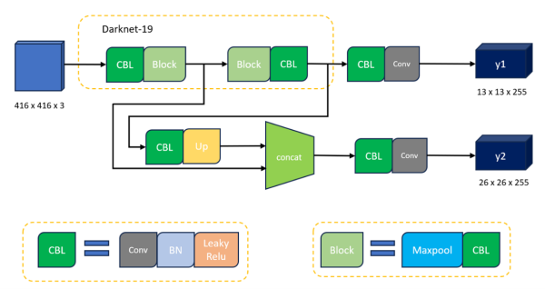
Here, we present a defect detection solution using the tiny variation of the You Only Look Once, Version 3 (YOLOv3-tiny) deep learning algorithm. YOLOv3-tiny is a lightweight object detection algorithm. The network structure of YOLOv3-tiny is as follows.
Compared with the original YOLOv3 model, YOLOv3-tiny reduces some layers and parameters to improve the inference speed and efficiency on embedded devices. The algorithm has high real-time performance and good accuracy, which is very suitable for industrial defect detection applications.
The defect detection solution can be deployed on RZ/V2L and RZ/V2M MPU chips. The deployment process is shown in the figure below.

ONNX is an open format built to represent machine learning models. ONNX defines a common set of operators - the building blocks of machine learning and deep learning models and a common file format to enable AI developers to use models with a variety of frameworks, tools, runtimes, and compilers.
The hardware setup of this application in the RZ/V2M MPU is as follows.

The hardware setup of this application in RZ/V2L MPU is as follows.

The YOLOv3-tiny defect detection solution is deployed on RZ/V2M and RZ/V2L. Low power consumption (less than 5W), has a high-performance inference effect, 52fps in RZ/V2M and 35fps in RZ/V2L (both don't include pre- and post-process).
Defect detection on the embedded side is not only used for PCB defect detection in electronic manufacturing, but it also has a wide range of application scenarios, the following are some common examples:
- Industrial automation: In manufacturing, defects in products such as incorrect product assembly, missing parts, or damage can be detected in real-time.
- Agricultural field: In agricultural production, it can be used to detect defects in crops or vegetables, such as diseases, insect pests, or fruit defects.
- Security monitoring: It can be used for defect detection in security monitoring systems, such as detecting abnormal objects, intrusion behaviors, or safety hazards in buildings or public places.
- Medical imaging: In the medical field, it can be applied to medical image analysis to detect disease markers, tumors or abnormal tissues, etc.
- Vehicle detection: In intelligent transportation systems, it can be used for vehicle detection, such as traffic flow monitoring, illegal vehicle detection, or parking lot management.
With the continuous advancement of artificial intelligence technology, we look forward to launching more applications and solutions in many fields such as industrial manufacturing, security, smart retail, server robots, etc.

