In today's rapidly evolving technology market, the demand for faster, more efficient product development is higher than ever. Businesses are constantly seeking ways to streamline their processes and reduce time-to-market. Products that help save time, simplify design, and cut costs are essential to staying competitive.
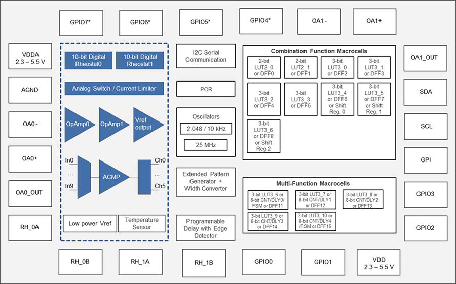
The Renesas AnalogPAK™ SLG47001/03 is designed to meet this demand by combining critical analog and digital functions into a single integrated circuit, effectively replacing multiple discrete components. Specifically, one SLG47001/03 consolidates two operational amplifiers (op amps), up to six analog comparators (ACMPs), and one analog switch into one compact unit. On top of that, it eliminates the need for up to eleven passive components, further simplifying the design. This sharp reduction in components translates into significant time savings during the development phase.
By eliminating the need to source, test, and validate separate components, the SLG47001/03 can cut weeks or even months off a typical development cycle. It comes with a manageable 8-week production lead time, ensuring that the design and manufacturing processes can be executed smoothly and without prolonged delays. Instead of managing numerous individual parts and ensuring their compatibility, engineers can now rely on a single, fully integrated solution. Not only does this speed up prototyping, but also streamlines manufacturing, reducing the number of sourcing and assembly steps.
The benefits extend beyond development time. With fewer components on the Bill of Materials (BOM), logistics become more straightforward, and the risk of supply chain disruptions is minimized. Fewer parts also reduce the potential for design errors, simplify troubleshooting, and improve overall product reliability. In addition, the SLG47001/03's integration leads to a smaller PCB footprint, reducing both production costs and power consumption, making it ideal for applications where space and energy efficiency are critical.
In a world where speed to market can make or break a product's success, the SLG47001/03 enables teams to move faster without sacrificing quality. By replacing numerous analog components with a single IC, it simplifies design, slashes the BOM, and accelerates time-to-market—giving businesses a clear competitive advantage.
For what technological solutions can the SLG47001/03 be used?
The SLG47001/03 is a programmable mixed-signal matrix with analog features, which can be configured for various applications, such as a gas sensor analog front-end, a shunt current sensor, a tunable active filter, an analog front-end for the photodiode, a data acquisition system, a low-power programmable gain amplifier, thermal protection with trimmable threshold, and more.
What is inside the SLG47001/03?

It is two zero-drift and ultra-low offset Operational Amplifiers that are the heart of the SLG47001/03. These op amps with rail-to-rail input and output (RRIO) work with signals of a large dynamic range. This is particularly useful in applications requiring high accuracy and low noise, such as measuring devices, medical devices, and sensor systems.
In addition, the SLG47001/03 contains two 10-bit (1024 taps) Digital Rheostats, which can be reconfigured in potentiometer mode. The value of Rheostats can be changed via I²C, internal logic, or extended pattern generator (preset values). When it comes to measurements and filtering, SLG47001/03's digital rheostats are all that you need for precise resistance adjustments.
The next crucial block is the Multichannel Sampling ACMP, which replaces up to six precise analog comparators. This macrocell is highly configurable and can work in analog MUX optional mode. It is possible to compare one channel with up to six different reference voltages. Thanks to its features, this macrocell is specifically designed to be a part of customer protection applications. One of the examples is the bidirectional current monitor, where you get current signal amplification, overvoltage, undervoltage, and overcurrent with low and high threshold protections.
The set also includes the Extended Pattern Generator with a width converter mode, which can generate complex digital patterns and sequences. The data width is 59 bytes with an optional 8-bit output to digital rheostats. In the width converter mode, 8-bit data can be divided into two 4-bit words, four 2-bit words, or a serial bit stream. The most noticeable advantage is the variety of applications that can be created using this block: SPI master transactions generation, pulse code modulated signal generation, RGB LEDs control (address LEDs and traditional LEDs), long 1-bit pattern generation (up to 472 bits), I²C master transactions generation, UART master transactions generation, 1-wire transactions generation, PWM signal generation (up to eight 8-bit channels), and more.
Moreover, the SLG47001/03 is equipped with power-saving features for all blocks, reliable NVM CRC check control, and GreenPAK™ configurable logic. Make sure to check out our free GUI-based Go Configure™ Software Hub to create your own designs in just a few minutes.
Summarizing all the above, the SLG47001/03 is the perfect choice for signal processing and data management.
Save your time without neglecting quality. Read more about AnalogPAK from Renesas to choose the SLG47001 or SLG47003 for your next project.
View our Application Notes for ready design examples.
Order an SLG47001V-SKT, SLG47003V-SKT, SLG47003V-DIP, or SLG47003-DMO board to begin evaluation.
