概要
説明
The 841654I is an optimized PCIe and sRIO clock generator. The device uses a 25MHz parallel crystal to generate 100MHz and 125MHz clock signals, replacing solutions requiring multiple oscillator and fanout buffer solutions. The device has excellent phase jitter (< 1ps rms) suitable to clock components requiring precise and low-jitter PCIe or sRIO or both clock signals. Designed for telecom, networking and industrial applications, the 841654I can also drive the high-speed sRIO and PCIe SerDes clock inputs of communication processors, DSPs, switches and bridges.


特長
- Four differential HCSL clock outputs: configurable for PCIe (100MHz) and sRIO (100MHz or 125MHz) clock signals One REF_OUT LVCMOS/LVTTL clock output
- Selectable crystal oscillator interface, 25MHz, 18pF parallel resonant crystal or LVCMOS/LVTTL single-ended reference clock input
- Supports the following output frequencies:
100MHz or 125MHz - VCO: 500MHz
- PLL bypass and output enable
- RMS phase jitter at 100MHz, using a 25MHz crystal (1.875MHz - 20MHz): 0.44ps (typical)
- Full 3.3V power supply mode
- -40°C to 85°C ambient operating temperature
- Available in lead-free (RoHS 6) package
製品比較
アプリケーション
設計・開発
モデル
ECADモデル
[製品選択]テーブル内の製品名をクリックするとSamacSysが提供する回路図シンボル、PCBフットプリント、3D CADモデルがご確認いただけます。 お探しのシンボルやモデルが見つからない場合、Webサイトから直接リクエストできます。

Processing table
| TSSOP | 28 | Tube | 3 | 0 | 48 | Yes | e3 Sn | -40 to +85°C | ||
| TSSOP | 28 | Reel | 3 | 1000 | 0 | Yes | e3 Sn | -40 to +85°C |
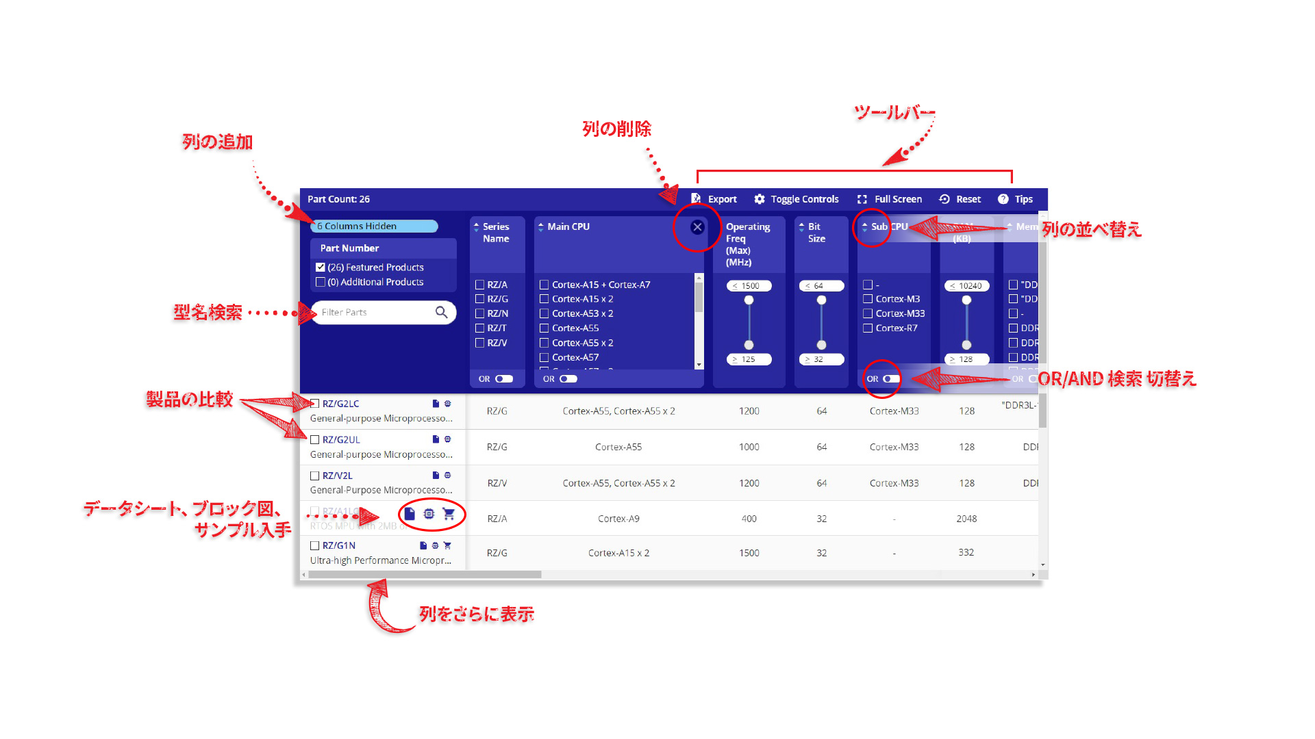
Tips for Using This Parametric Table:
- Hide Filters button in header: Collapse or expands filters
- Column sort buttons in header: Sort Column alphabetically / numerically descending or ascending
- Reset button in header: Reset all filters to the page default
- Full Screen button in header: Expand the table to full screen view (user must close out of full screen before they can interact with rest of page)
- Export button in header: Export the filtered results of the table to an Excel document
- Filter parts search bar in header: Type to filter table results by part number
- Hide column button in column headers: Select to hide columns in table
- AND / OR toggle switches in header: Toggles the logic of this particular filter to be “AND” or “OR” logic for filtering results
- Multiselect checkboxes at beginning of each row in table: Select these checkboxes to compare products against each other
- Document icon next to product name in row: View the featured document for this product
- Chip icon next to the right of the document icon in row: View the block diagram for this product
- Cart icon to the right of the chip icon: Indicates that samples are available for this product