概要
説明
The 8V34S208 is a differential 1:8 LVDS fanout buffer with a 2:1 input multiplexer. The device accepts DC to 250MHz clock and data signals and is designed for 1Hz clock/1PPS, 2kHz, and 8kHz signal distribution. Controlled by the input mode selection pin, the differential input stages accept both rectangular or sinusoidal signals. The 8V34S208 also provides level-translated LVCMOS/LVTTL outputs which are copies of the individual differential inputs CLKA and CLKB. The propagation delay of the device is very low, providing an ideal solution for clock distribution circuits with tight phase alignment requirements. The multiplexer select pin (SEL) allows the selection of one out of two input signals, which is copied to the four differential outputs.


特長
- Designed for 1PPS, 2kHz, 8kHz, and 10MHz GPS clock signal distribution
- High-speed 1:8 LVDS fanout buffer
- Eight differential LVDS output pairs
- 2:1 input multiplexer
- Two selectable differential inputs accept LVDS and LVPECL signals
- Accepts rectangular and sinusoidal input signals
- Two input monitoring outputs (LVCMOS)
- Max output frequency: 250MHz
- Additive RMS phase jitter: 118fs (typical) at 100MHz (12kHz to 20MHz)
- Part-to-Part skew: 250ps (maximum)
- Propagation delay: 325ps (typical), LVDS output
- Full 2.5V and 3.3V voltage supply
- -40 °C to 85 °C ambient operating temperature
- Lead-free 32-lead VFQFN (RoHS 6/6) packaging
製品比較
アプリケーション
設計・開発
モデル
ECADモデル
[製品選択]テーブル内の製品名をクリックするとSamacSysが提供する回路図シンボル、PCBフットプリント、3D CADモデルがご確認いただけます。 お探しのシンボルやモデルが見つからない場合、Webサイトから直接リクエストできます。

Processing table
| VFQFPN | 32 | Tray | 3 | 0 | 490 | Yes | e3 Sn | -40 to +85°C | ||
| VFQFPN | 32 | Reel | 3 | 2500 | 0 | Yes | e3 Sn | -40 to +85°C |
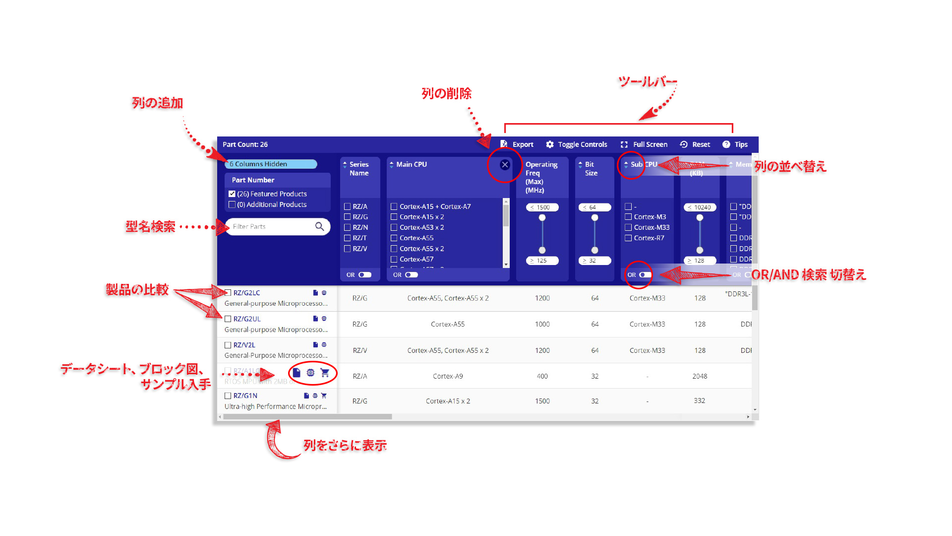
Tips for Using This Parametric Table:
- Hide Filters button in header: Collapse or expands filters
- Column sort buttons in header: Sort Column alphabetically / numerically descending or ascending
- Reset button in header: Reset all filters to the page default
- Full Screen button in header: Expand the table to full screen view (user must close out of full screen before they can interact with rest of page)
- Export button in header: Export the filtered results of the table to an Excel document
- Filter parts search bar in header: Type to filter table results by part number
- Hide column button in column headers: Select to hide columns in table
- AND / OR toggle switches in header: Toggles the logic of this particular filter to be “AND” or “OR” logic for filtering results
- Multiselect checkboxes at beginning of each row in table: Select these checkboxes to compare products against each other
- Document icon next to product name in row: View the featured document for this product
- Chip icon next to the right of the document icon in row: View the block diagram for this product
- Cart icon to the right of the chip icon: Indicates that samples are available for this product