概要
説明
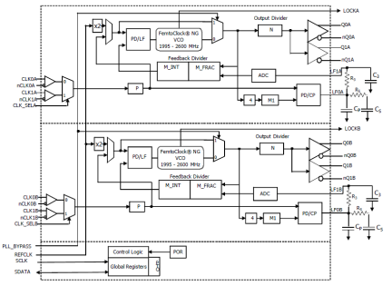
The 8T49N244I is a dual PLL using FemtoClock® NG technology. It integrates low phase noise frequency translation/synthesis and jitter attenuation. The device includes alarm and monitoring functions suitable for networking and communications applications. It has two fully independent PLLs. Each PLL can generate any output frequency in the 0.98MHz to 312.5MHz range and most output frequencies in the 312.5MHz to 1,300MHz range. A wide range of input reference clocks may be used as the source for the output frequencies.
Each PLL has three operating modes to support a very broad spectrum of applications: Frequency Synthesizer, High-Bandwidth Frequency Translator, and Low-Bandwidth Frequency Translator.
特長
- Fourth-generation FemtoClock NG technology
- Two fully independent PLLs
- Outputs are programmable as LVPECL or LVDS
- Programmable output frequency: 0.98MHz up to 1,300MHz
- Two differential inputs support the following input levels: LVPECL, LVDS, LVHSTL, HCSL
- Input frequency range: 8kHz to 710MHz
- Input clock monitor and alarm
- Smoothed reference switch
- I²C serial interface for register programming
- RMS phase jitter: 486fs (typical), Low Bandwidth Mode (FracN)
- RMS phase jitter: 326fs (typical), Synthesizer Mode (Integer FB)
- Full 2.5V ± 5% supply mode
- -40 °C to 85 °C ambient operating temperature
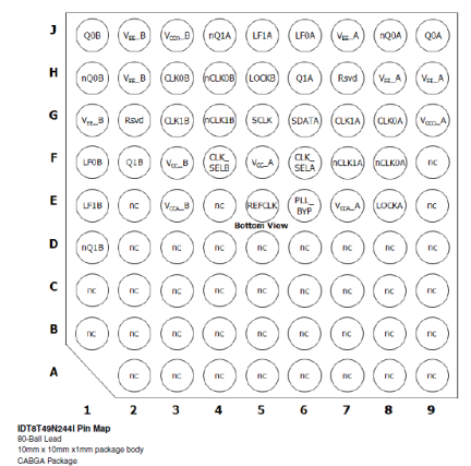
- 10mm x 10mm CABGA lead-free (RoHS 6) package
- Additional family members include Tri-PLL (8T49N366I) and Quad PLL (8T49N445I and 8T49N488I) devices
製品比較
アプリケーション
設計・開発
モデル
ECADモデル
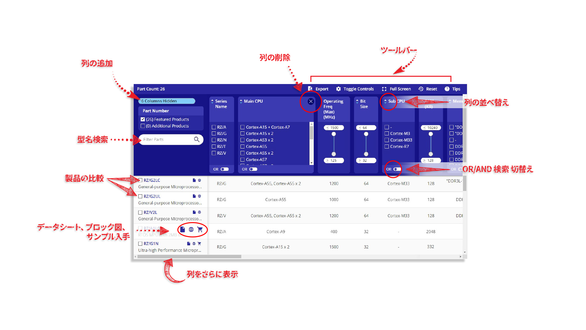
[製品選択]テーブル内の製品名をクリックするとSamacSysが提供する回路図シンボル、PCBフットプリント、3D CADモデルがご確認いただけます。 お探しのシンボルやモデルが見つからない場合、Webサイトから直接リクエストできます。


